Net ties, star routing and decoupling capacitors as first-level tool

Bug #1571930 reported by Simon Richter
86
This bug affects 17 people
Affects Status Importance Assigned to Milestone
KiCad
Expired
Wishlist

Bug Description

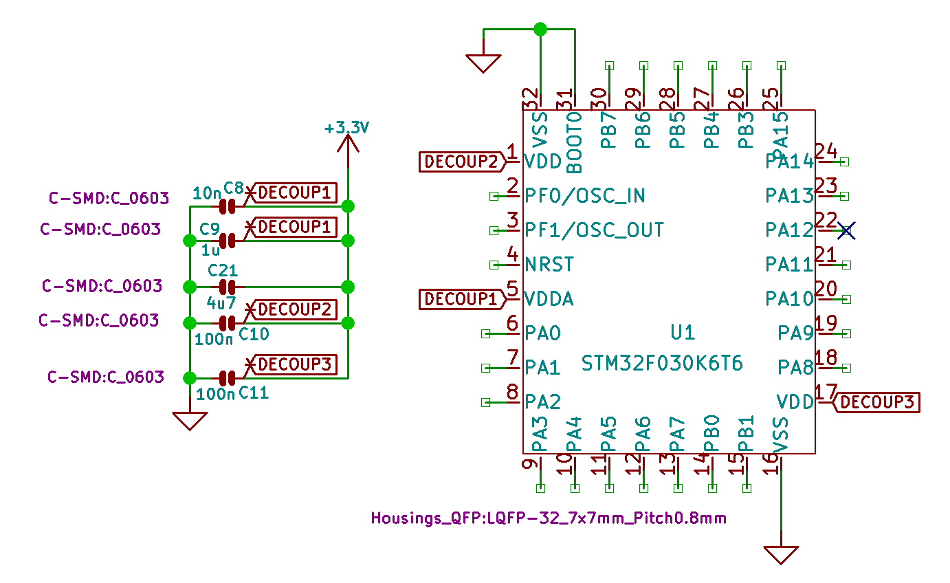
These three features are similar in type:

 - net ties connect two different nets in one place only.
 - star routing requires certain traces to start either on a specific pad or at a common point (like a single-layer via)
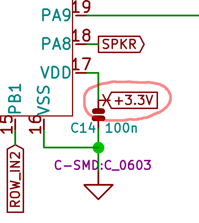
 - decoupling capacitors should be connected to certain pins primarily

All of these modify ratsnest and DRC behaviour. Ratsnest would be correct if these nets were distinct (giving DRC errors), and DRC would be correct if the nets were the same (giving wrong ratsnest), so explicitly communicating requirements would be good here.

Simon Richter (sjr)
Changed in kicad:
status: New → In Progress
Revision history for this message
Evan Shultz (evan-shultz) wrote :

Thanks Simon! I don't see a native way to make star net/ground connections, and it's sorely needed. There must be a method to join together two nets only at a specific point in the PCB.

One note is that an IPC-356 netlist has a section for net shorts and the solution should be sure to take advantage of it. Otherwise the netlist will not match the board and contain "unintended" shorts.

Revision history for this message
Novak Tamas (novak-7) wrote :

It is an *important* wish, as high pin-count packages have a lot of Vdd's with decoupler 100nF's on each, plus some pins pulled-up, so you need to focus where to place decouplers.

Revision history for this message
jean-pierre charras (jp-charras) wrote :

For me net ties and decoupling capacitors are two different and unrelated things.
Both are important, but are different features.

* Net ties are related to netlist management.
* Decoupling capacitors are related to routing constraints management.
This is very different.

I am not sure decoupling capacitors constraints must be fixed at schematic level (at least from the point of view of efficiency), although fixing these constraints at schematic level has an interest: it open the door to an automatic placement of decoupling capacitors.

On the other hand, fixing these constraints at schematic level could creates a lot more work than just made a good layout by a skilled designer, without ensure there is no error.

Revision history for this message
Evan Shultz (evan-shultz) wrote :

I also feel they're different, but I see them as related.

Star ground connections serve a purpose that can't be handled any other way (though there are many ways to implement stars in a design). When I want a common logical connection between nets/grounds, but require a specific placement of the net/ground connection, then I must have a star ground/net location which I can place and/or control (star net/ground part, property on a pin/via/etc. that allows shorting at that one element, etc.).

Decoupling capacitors, at least in my experience, are able to be reasonably managed within the tool as-is. That being said, I do see how a star net/ground could help here to ensure that a given capacitor can only be connected across one specific pin. But as JP says, just being cognizant can handle this already. Or perhaps there's a perspective on this I'm not seeing?

Revision history for this message
Simon Richter (sjr) wrote : Re: [Bug 1571930] Re: Net ties, star routing and decoupling capacitors as first-level tool

Hi,

On 08.07.2016 20:28, jean-pierre charras wrote:

> For me net ties and decoupling capacitors are two different and unrelated things.
> Both are important, but are different features.

Indeed. The schematic would probably not use a "net tie" tool for that,
because it doesn't enhance readability at all, and it would be a lot of
work to create the schematic.

In the board layout however, the functionality required for decoupling
capacitors and for net ties is so similar that it makes sense to treat
them the same.

> * Net ties are related to netlist management.
> * Decoupling capacitors are related to routing constraints management.
> This is very different.

Net ties are a mixture of both -- technically, digital and analog ground
are connected by copper, so you could argue that they're the same net,
and the only difference between them is a routing constraint.

> I am not sure decoupling capacitors constraints must be fixed at
> schematic level (at least from the point of view of efficiency),
> although fixing these constraints at schematic level has an interest: it
> open the door to an automatic placement of decoupling capacitors.

I think that it would be nice to have a "table" schematic element for
things like this -- the table would be printed on the sheet it is placed
on as text, and netlist items can be created from it. This could also be
used for the power supply pins on logic gates -- the table would list
the hidden pins and the nets they are connected to.

> On the other hand, fixing these constraints at schematic level could
> creates a lot more work than just made a good layout by a skilled
> designer, without ensure there is no error.

I'm certainly not a skilled designer, so I try to add functions to help
me catch errors early.

   Simon

Revision history for this message
jean-pierre charras (jp-charras) wrote :

Anything is a routing constraint.

I maintain Net ties and decoupling capacitors are very different cases:

The purpose of a net ties is mainly to separate 2 nets during routing.
(Not necessary 2 ground: there are many other cases)

Decoupling capacitors do not need net tee.
They need only a constraint: max distance between they pin x and the pin y of the component to decouple (which is not always a power net).
This is the only one constraint you have for decoupling capacitors, from the point of view of board design.

Net ties do not create such a constraint and are therefore useless for decoupling capacitors management.

Revision history for this message
Novak Tamas (novak-7) wrote :

Decoupler capacitor case may not be regarded as a distance constraint.
If a "this pin is part of net1, while also the member of net2" function was implemented (this info must be registered somehow both in .sch and netlist), it worked like this:

In case of decouplers,
1 - make a connection between C (capacitor pin) and P (one Vdd pin of the package): net1
2 - select C pin, and click the new "net tie" tool
3 - select the net connecting to (net2). Only from a list of named nets (no "Net-(P3-Pad2)" kinda names interested) like PWR_GND, +3.3V etc. Selecting graphically (the whole net highlite while hovering over) would be nice, but not necessary.

In pcb_new all functions (ratsnests, Add/edit track, Highlight net..) work according to
- pin P only connects to pin C
- pin C connects to pin P and all pins of net2
- net2 pins connect to all net2 pins and C

Star topology, decouplers, and "two nets connecting at a given point" could be created this way.

Revision history for this message
Simon Richter (sjr) wrote :

Hi,

On 09.07.2016 08:18, jean-pierre charras wrote:

> I maintain Net ties and decoupling capacitors are very different cases:

I agree -- decoupling capacitors cannot be fully solved with net ties.

The main difficulty I have in the layout of the capacitors is not
distance, but knowing which capacitor belongs to which pin. If I place a
net tie between the power rail on one side, and the capacitor and the IC
pin on the other, the ratsnest line will connect each pin to its
capacitor, which would be a marked improvement.

> They need only a constraint: max distance between they pin x and the pin y of the component to decouple (which is not always a power net).
> This is the only one constraint you have for decoupling capacitors, from the point of view of board design.

Yes, length and loop area constraints would be really great to have as
well, and we could also translate these into a usable ratsnest (length
constrained connections will always be drawn, even if another ratsnest
line would be shorter).

I think I can set up a blueprint for that as well once the wiki goes live,

   Simon

Revision history for this message
Simon Richter (sjr) wrote :

Hi,

On 10.07.2016 11:52, Novak Tamas wrote:

> Decoupler capacitor case may not be regarded as a distance constraint.

The answer is somewhere in the middle. It would be nice to have distance
and loop area constraints, but I won't touch that until net ties are done.

JP has identified the main problem with net ties though -- we don't know
how the layouter wants to do the connections. With the "net ties as
ratsnest anchors" approach I favour, this should be doable:

1. via - trace - capacitor - trace - ic

Place the net tie on the capacitor pad.

2. via in capacitor pad - trace - ic

Place the net tie either on the via or on the capacitor pad.

3. capacitor - trace - via - trace - ic

Place the net tie on the via.

4. capacitor - trace - via in ic pad

Place the net tie either on the via or on the ic pad.

With Altium style net ties, that doesn't work.

I've been writing a lengthy document about this, I'm just waiting for
the official developer wiki to open so I can publish it.

> If a "this pin is part of net1, while also the member of net2" function was implemented (this info must be registered somehow both in .sch and netlist), it worked like this:

Checking against known use cases:

1. analog/digital ground: doesn't work, no pins involved
2. shunt resistors: solved nicely
3. decoupling caps: unclear whether we win much here
4. length matching: doesn't work, pins on the wrong side

> In case of decouplers,
> 1 - make a connection between C (capacitor pin) and P (one Vdd pin of the package): net1
> 2 - select C pin, and click the new "net tie" tool
> 3 - select the net connecting to (net2). Only from a list of named nets (no "Net-(P3-Pad2)" kinda names interested) like PWR_GND, +3.3V etc. Selecting graphically (the whole net highlite while hovering over) would be nice, but not necessary.

How would you represent that in the schematic? Keep in mind that
anything that goes into the netlist needs to be obvious when you look at
the schematic.

   Simon

Revision history for this message
jean-pierre charras (jp-charras) wrote :

This topic should be moved to the dev. mailing list.

Revision history for this message
Novak Tamas (novak-7) wrote :

>How would you represent that in the schematic? Keep in mind that
>anything that goes into the netlist needs to be obvious when you look at
>the schematic.

What if net tie can be done only by a new kinda label ("net tie label") not by placing wires.
This wire can be placed on on pins (see picture attached). Label text must be the net name of an existing net.

Revision history for this message
Novak Tamas (novak-7) wrote :

This wire can be placed on on pins (see picture attached).

*** This label can be placed on pins only

(The only thing about me I type very quickly:)))

Revision history for this message
Evan Shultz (evan-shultz) wrote :
Download full text (5.2 KiB)

@Novak Tamas If only a label is used to indicate a net tie, what is the physical implementation? How does the designer specify the location on the PCB where the nets are joined? While there may be a good solution that is abstract, like a table or property, I wonder if an actual component is better simply because of legacy/continuity with other software so users will already know what to do with less documentation/explanation?

To educate myself I installed eval versions of the big, commercial ECAD tools to see what they do regarding net ties. Along with searching online and reading the help files, I made a minimal design to show the net tie feature; it's entirely possible that I didn't find the correct/best way to perform net ties in the various tools so please share if you have thoughts.

My criteria for success is the fundamental requirement of a net tie: join 2 or more nets at a specific point on the PCB, without creating intrinsic DRC errors, and with a "correct" netlist file. I've used a multi-pin component which had a non-Cu line that was Gerber'd out to the appropriate copper layer. A place keepout and route keepout was located between the pins so that the user couldn't create an unexpected short with the copper that would appear in the physical board. This worked, but there were always issues with the part not being used properly and the netlist not showing the net shorts which needed to be manually mentioned to the fab house. It was a big pain. I believe this type of implementation is possible in every PCB design tool, but since it's generally prone to broken manufacturing outputs or generates unavoidable DRC errors I'm not considering it as a solution.

Below you'll find a more detailed explanation of what I found in each tool, but here's the summary: to me Allegro is the winner as it's easy and flexible. It doesn't require a schematic implementation, but supports it if desired. Zuken and Altium are pretty close in designing with the net tie, but get demerits by not showing the short in an IPC-356 netlist. PADS is loses because even though it handles the netlist issue nicely it's limited in how, and how easily, the board can be designed.

Cadence Allegro PCB Designer (DE-CIS or DE-HDL + Allegro 16.6-2015)
Allegro supports a special net_short property on a schematic or PCB pin which allows those nets to be shorted at the pin. The property syntax is "net_short = <net1>:<net2>:<net3>...". A DRC error will be created a for net short during routing, even during routing the trace to the pin, but after placing the trace the error will be supposed. Zones can be used in place of traces. The route must start at the first net in the net_short sequence and go to the later nets (routing it backwards will leave the DRC error). Because there need not be a schematic component, if the nets are changed in the schematic the property must be updated in the board; conversely, a schematic component can be created with the property already added for common net shorts, like between AGND and DGND. Generating an IPC-356 netlist has a special section where net shorts are shown. Here's an overly complicated explanation using the CIS front-end (it can be done s...

Read more...

Revision history for this message
Novak Tamas (novak-7) wrote :

What I think of: (please see attached image)

New type "net tie label" must be placed to a pin, not anywhere on a net. It connects the actual pin to a net, and gives no DRC error if this causes joining two (or more) different nets.
This may work as local label (these net ties must be within the same schema/hierarchy level).

Decoupler case:
DECOUP1 is a normal net, containing 3 pins. The ratsnest for these (C8 right, C9 right, U1/pin5) is normally handled: from U1/5 a ratsnest line goes to C8 or C9 (which is closer), then further to the other capacitor.
An independent ratsnest for +3.3V connects C8,C9,C10,C11,C21 in any order, as usual. (The label on U1/5 may be even a normal local label, as it is member of a single net only). The speciality is only that no DRC error for e.g. C8 right side, where to different nets (+3.3V and DECOUP1) are interconnected.

Net tie case:
You need a single pin component as star point. It also may have a single pad footprint. Two normal nets exist (e.g AGND and DGND. If they are not named yet, place a local label on them). Then you put two "net tie labels" on starpoint component both for AGND and DGND.

Revision history for this message
Wayne Stambaugh (stambaughw) wrote :
Download full text (5.8 KiB)

On 7/27/2016 6:14 PM, Evan Shultz wrote:
> @Novak Tamas If only a label is used to indicate a net tie, what is the
> physical implementation? How does the designer specify the location on
> the PCB where the nets are joined? While there may be a good solution
> that is abstract, like a table or property, I wonder if an actual
> component is better simply because of legacy/continuity with other
> software so users will already know what to do with less
> documentation/explanation?
>
> To educate myself I installed eval versions of the big, commercial ECAD
> tools to see what they do regarding net ties. Along with searching
> online and reading the help files, I made a minimal design to show the
> net tie feature; it's entirely possible that I didn't find the
> correct/best way to perform net ties in the various tools so please
> share if you have thoughts.
>
> My criteria for success is the fundamental requirement of a net tie:
> join 2 or more nets at a specific point on the PCB, without creating
> intrinsic DRC errors, and with a "correct" netlist file. I've used a
> multi-pin component which had a non-Cu line that was Gerber'd out to the
> appropriate copper layer. A place keepout and route keepout was located
> between the pins so that the user couldn't create an unexpected short
> with the copper that would appear in the physical board. This worked,
> but there were always issues with the part not being used properly and
> the netlist not showing the net shorts which needed to be manually
> mentioned to the fab house. It was a big pain. I believe this type of
> implementation is possible in every PCB design tool, but since it's
> generally prone to broken manufacturing outputs or generates unavoidable
> DRC errors I'm not considering it as a solution.
>
> Below you'll find a more detailed explanation of what I found in each
> tool, but here's the summary: to me Allegro is the winner as it's easy
> and flexible. It doesn't require a schematic implementation, but
> supports it if desired. Zuken and Altium are pretty close in designing
> with the net tie, but get demerits by not showing the short in an
> IPC-356 netlist. PADS is loses because even though it handles the
> netlist issue nicely it's limited in how, and how easily, the board can
> be designed.
>
> Cadence Allegro PCB Designer (DE-CIS or DE-HDL + Allegro 16.6-2015)
> Allegro supports a special net_short property on a schematic or PCB pin which allows those nets to be shorted at the pin. The property syntax is "net_short = <net1>:<net2>:<net3>...". A DRC error will be created a for net short during routing, even during routing the trace to the pin, but after placing the trace the error will be supposed. Zones can be used in place of traces. The route must start at the first net in the net_short sequence and go to the later nets (routing it backwards will leave the DRC error). Because there need not be a schematic component, if the nets are changed in the schematic the property must be updated in the board; conversely, a schematic component can be created with the property already added for common net shorts, like between AGND and DGND. G...

Read more...

Jeff Young (jeyjey)
Changed in kicad:
status: In Progress → Triaged
Revision history for this message
Simon Richter (sjr) wrote :

This is still in progress here, or at least I keep rebasing the branch containing the fragments in the hope of ever making progress.

Jeff Young (jeyjey)
Changed in kicad:
status: Triaged → In Progress
Revision history for this message
Hildo Guillardi Júnior (hildogjr) wrote :

@Jeff, some advance in this issue?
Someone just post a duplicated https://bugs.launchpad.net/kicad/+bug/1846832

Revision history for this message
Jeff Young (jeyjey) wrote :

@Hildo, @Simon is working on it. (My expertise is in software so this is a bit over my pay grade.)

Revision history for this message
Timo Alho (tisaalho) wrote :

As a quick comment, one more use case (which has been implied but not mentioned explicitly in this thread) is net ties on inner layers, which is quite a big deal for mixed-signal design. See https://electronics.stackexchange.com/questions/471567/kicad-net-tie-on-inner-layer for my current use case.

Also, if this is coming as a full feature only in 6.0, it would be very nice to have some kind of a workaround/hack before that which doesn't give persistent errors (so the hack mentioned in https://forum.kicad.info/t/footprints-pads-on-internal-layers/11214/21 doesn't quite work, though just removing the error messages and making the inner pads visible might be enough to make this tolerable, as mentioned in the thread).

For my specific use case, a possible nice first class implementation could be that the net tie would actually appear as a special zone in pcbnew (obviously also somehow visible in eeschema), which would be allowed to connect to two different zones (and would then generate the corresponding short in the netlist too). This would allow drawing the connection on the PCB in whichever shape appears most useful once the routing gets underway. Unfortunately I don't have the time to analyze right now how this would affect the other use cases mentioned in this thread.

Revision history for this message
Maciej Suminski (orsonmmz) wrote :

Hi Timo,

We have recently moved to Gitlab. You can follow your bug report here: https://gitlab.com/kicad/code/kicad/issues/2018

Revision history for this message
KiCad Janitor (kicad-janitor) wrote :

KiCad bug tracker has moved to Gitlab. This report is now available here: https://gitlab.com/kicad/code/kicad/-/issues/2018

Changed in kicad:
status: In Progress → Expired
To post a comment you must log in.
This report contains Public information  
Everyone can see this information.

Other bug subscribers

Remote bug watches

Bug watches keep track of this bug in other bug trackers.