Footprint Editor Lacks Edge.Cuts Layer
| Affects | Status | Importance | Assigned to | Milestone | |
|---|---|---|---|---|---|
| KiCad |
Expired
|
Wishlist
|
|||
Bug Description
I am designing a board with an edge connector the same as shown on the left side of this board:
http://
This edge connector is for plugging into a Silicon Labs ToolStick Base Adapter:
http://
So I will not have to design this repeatedly for every board I need this connector on, I am creating a module for it. In this module I will need to define the edge of the board where this edge connector is to be. But the Module Editor does not allow this because it lacks the option to put graphic lines in the Edge.Cuts layer.
In the Module Editor I need to be able to put a graphic line in the Edge.Cuts layer just as can be done in the PCB editor.

| Lorenzo Marcantonio (l-marcantonio) wrote : Re: [Bug 1251393] [NEW] Module Editor Lacks Edge.Cuts Layer | #1 |
| Stephen (artist-wavenet) wrote : Re: Module Editor Lacks Edge.Cuts Layer | #2 |
To get the graphic lines I needed in the Edge.Cuts layer I edited the module in a text editor and changed the layer code, the last number in the line that defines where the line is, to 28. If it can be done in the text editor is it really that difficult to set the number to 28 in KiCad software? :)
| Lorenzo Marcantonio (l-marcantonio) wrote : Re: [Bug 1251393] Re: Module Editor Lacks Edge.Cuts Layer | #3 |
On Fri, Nov 15, 2013 at 05:07:11AM -0000, Stephen Pflanze wrote:
> To get the graphic lines I needed in the Edge.Cuts layer I edited the
> module in a text editor and changed the layer code, the last number in
> the line that defines where the line is, to 28. If it can be done in the
> text editor is it really that difficult to set the number to 28 in KiCad
> software? :)
Don't come here if something else (like DRC or zone filling) break,
then! In fact there is an *explicit* exclusion in that code path.
--
Lorenzo Marcantonio
Logos Srl
| Stephen (artist-wavenet) wrote : Re: Module Editor Lacks Edge.Cuts Layer | #4 |
Please add to this feature request the addition of the same "Add dimension" feature that is in the Pcbnew editor to the module editor. For this edge connector there are dimensions that needed to be in the documentation layer that I do not want to have to redo every time I add this connector to a board. So I used text and graphic line objects to do this in the Module editor. An "Add dimension" feature in the module editor would have saved me a lot of time.
| Changed in kicad: | |
| importance: | Undecided → Wishlist |
| summary: |
- Module Editor Lacks Edge.Cuts Layer + Footprint Editor Lacks Edge.Cuts Layer |
| tags: | added: modedit |
| tags: |
added: fpedit removed: modedit |
| Rene Poeschl (poeschlr) wrote : | #5 |
Could someone add a reason as what the problem is with edge cuts in footprints?
Currently we already have some footprints that have the edge cut defined in the official library. Should we remove them (or move these drawings to a different layer)?
| Wayne Stambaugh (stambaughw) wrote : Re: [Bug 1251393] Re: Footprint Editor Lacks Edge.Cuts Layer | #6 |
AFAIK, pcbnew does not merge edge cuts in footprints with the edge cuts
in the board so a complete board outline is not generated. Someone
please correct me if I'm wrong about this. It is a known issue and
hopefully we will get it resolved in v6. As for moving edge cut layers
in footprints, you could move them to a fab layer so the user can use
the outline to copy to the edge cut layer on the board.
On 2/13/2018 1:57 PM, Rene Poeschl wrote:
> Could someone add a reason as what the problem is with edge cuts in footprints?
> Currently we already have some footprints that have the edge cut defined in the official library. Should we remove them (or move these drawings to a different layer)?
>
| jean-pierre charras (jp-charras) wrote : | #7 |
In fact Pcbnew takes in account edge cuts in footprints (at least plot files and when builds the board outlines).
The reason edge cuts are not allowed is due to:
1 - board outline must be a closed simple polygon (for 3D view, for DSN export and to have a well defined outline to make the board.
2 - holes created by edge cuts are allowed in boards, but for the same reasons, they should be simple polygons, non intersecting between them and the main outline.
Otherwise you cannot really define the board shape.
3 - Edge cuts in footprints cannot safely meet these requirement, because they are created without knowledge of the board ( grid size for instance, and other footprints put on the board).
So, allowing edge cuts in footprints is a good way to create board outline issues.
| Nick Østergaard (nickoe) wrote : | #8 |
I don't quite understand why this should disallow users to create board outlines in the footprint. The same rules and issues apply for just defining the board outline in pcbnew directly.
| jean-pierre charras (jp-charras) wrote : | #9 |
"The same rules and issues apply for just defining the board outline in pcbnew directly"
Not really true.
As I said previously, a board outline has constraints.
When you create the board outline, you know the grid size, and you are able to create a closed polygon.
This is not the case when creating a footprint.
Some time ago, creating edge cuts in footprints was allowed.
The main result was bug reports about not closed board outlines.
What is the interest to allow things in pcbnew, when these things are broken?
| Wayne Stambaugh (stambaughw) wrote : | #10 |
On 2/14/2018 7:04 AM, jean-pierre charras wrote:
> "The same rules and issues apply for just defining the board outline in
> pcbnew directly"
>
> Not really true.
By "same rules" I meant a fully enclosed board outline. Whether an edge
cut is defined in the board or on in a footprint, the board outline
created by combining all of the edge cut geometry still has to be
enclosed. Are there any other constraints that I am missing?
>
> As I said previously, a board outline has constraints.
>
> When you create the board outline, you know the grid size, and you are
> able to create a closed polygon.
>
> This is not the case when creating a footprint.
>
> Some time ago, creating edge cuts in footprints was allowed.
> The main result was bug reports about not closed board outlines.
I always felt this issue was due to a lack of proper tools in pcbnew.
Once we have segment snapping implemented in the modern canvas, this
issue should be mitigated. You can still draw a board outline that is
not fully enclosed even if you don't use edge cuts from footprints.
Perhaps a DRC check to test for closed board outline polygon would be
useful.
>
> What is the interest to allow things in pcbnew, when these things are
> broken?
>
The only reasonable way to create edge connector footprints is to draw
the board edge along with the pads to ensure the correct spacing and
alignment. There are other footprint that require board cutouts to be
correctly located.
| Rene Poeschl (poeschlr) wrote : | #11 |
If i read your comments correctly then the only reason to disallow them is because it might create polygons that are not valid.
We could add a KLC rule requiring the edge cut to end on a fairly coarse grid that would allow users to connect them easily. (Similar what we do with pins for eeschema)
But this does not explain why opening a footprint with an edge cut currently moves the edge cuts lines to some other layer. This might be a step too far.
To justify that behavior i would expect something major to break when using footprints that use edge cuts.
---
The fab layer is not the right alternative either as it is intended for communicating with the fab. Not with the user of the footprint. You probably don't want this information stuck in your documentation either as the edge cuts layer already contains that info at that point.
The user.dwgs layer and comments layer might be better but these are also disallowed. But that is a different wishlist bug and beside the point here.
| jean-pierre charras (jp-charras) wrote : | #12 |
" Are there any other constraints that I am missing"
No.
"Whether an edge cut is defined in the board or on in a footprint, the board outline created by combining all of the edge cut geometry still has to be enclosed":
This is The Constraint: the full board outline must be a set of polygons (a board can have holes) not self intersecting and not intersecting, and with only one main outline.
This constraint is due to the fact you cannot define (without this constraint) what is inside a board and what is outside the board.
| jean-pierre charras (jp-charras) wrote : | #13 |
@Rene,
yes, the main reason to disallow them is because it probably create polygons that are not valid.
KLC rule cannot really fix that: if the segments are created on a grid on mm, and the footprint put on a grid in inches, it will be not so easy to create a good board outline.
However the algorithm that recreates outline polygons from segments and arcs needs only segment (or arcs) ends that are near, but not exactly at the same coordinate.
Think also a outline is not necessary the main outline: it can be a hole inside the board.
| Rene Poeschl (poeschlr) wrote : | #14 |
What i get from this discussion is: If done right there is no problem with using edge cuts in the footprint. (Which to me means: Yes we can use them and the current footprint editor behavior is at best sub-optimal.)
Footprints that define an internal cutout do not suffer from this problem at all. The same is true for footprints that define the complete outer board edge. (Both of these are usecases that are not possible currently without using a text editor to modify the footprint.)
By the way there is a bug requesting easy import of board edges [1] and the reason given for it being set to "Fix committed" is that footprint disambiguation no longer asks if a footprint defining the edge cut overlaps other footprints. (So either that bug is incorrectly set to fixed or the current footprint editor behavior is wrong.)
---
Fixing the grid in the KLC would allow users to know what grid to use for such footprints. (That grid requirement would only apply to footprints that have open ends to their edge cuts definition.) So it would make it easier for using such footprints.
If the user does use imperial grid they can edit the footprint to fit their personal needs. Like what should be done with any footprint found in the official library. We do not claim to have footprints that fit everyones needs but we try to find a "fits most usecases well enough" middle ground.
Again: I don't think this deficiency merits disallowing edge cuts in the footprint editor.
---
| Rene Poeschl (poeschlr) wrote : | #15 |
Maybe a step in the right direction would be to add the edge cuts layer similarly as the currently grayed out layers (Cmts, Dwgs, Eco, ...). And remove the automatic transfer of drawings on this layer.
This would allow users to view footprints with edge cuts defined and with enough determination to draw on it. (That would indirectly also communicate that there might be some dangers connected with using this layer.)
It would even allow for the usecase i mentioned above where a user of the imperial grid needs to modify the metric footprint found in the official library. (Currently this would result in the edge cut drawing being moved to some other layer. After the modification the user would need a text editor to get it back to the edge cuts layer.)
| jean-pierre charras (jp-charras) wrote : | #16 |
Yes, it is a sensible way to allow using edge cuts, and do no encourage this use, like for other, non paired, layers.
| Jeff Young (jeyjey) wrote : | #17 |
+1
> On 14 Feb 2018, at 17:40, jean-pierre charras <email address hidden> wrote:
>
> Yes, it is a sensible way to allow using edge cuts, and do no encourage
> this use, like for other, non paired, layers.
>
> --
> You received this bug notification because you are a member of KiCad Bug
> Squad, which is subscribed to KiCad.
> https:/
>
> Title:
> Footprint Editor Lacks Edge.Cuts Layer
>
> Status in KiCad:
> New
>
> Bug description:
> I am designing a board with an edge connector the same as shown on the left side of this board:
> http://
>
> This edge connector is for plugging into a Silicon Labs ToolStick Base Adapter:
> http://
>
> So I will not have to design this repeatedly for every board I need
> this connector on, I am creating a module for it. In this module I
> will need to define the edge of the board where this edge connector is
> to be. But the Module Editor does not allow this because it lacks the
> option to put graphic lines in the Edge.Cuts layer.
>
> In the Module Editor I need to be able to put a graphic line in the
> Edge.Cuts layer just as can be done in the PCB editor.
>
> To manage notifications about this bug go to:
> https:/
| Wayne Stambaugh (stambaughw) wrote : | #18 |
A few quick notes. Any changes should happen in v6. This would qualify
as a new feature and we are in feature freeze. Before we make any code
changes, we need to clearly define the behavior that we want so this
doesn't become an endless string of bug reports and patches. Depending
on how involved this behavioral change is, we could create a blueprint
to document the behavior and link it to this bug report so the developer
who takes on this task has clearly defined goals. I fine with a list of
clearly defined behaviors in the bug report if a blueprint is overkill.
On 2/14/2018 12:40 PM, jean-pierre charras wrote:
> Yes, it is a sensible way to allow using edge cuts, and do no encourage
> this use, like for other, non paired, layers.
>
| Changed in kicad: | |
| assignee: | nobody → jean-pierre charras (jp-charras) |
| status: | New → In Progress |
| jean-pierre charras (jp-charras) wrote : | #19 |
OK.
I'll postpone the fix until V6.
| Changed in kicad: | |
| milestone: | none → 6.0.0-rc1 |
| Frank Severinsen (shack) wrote : | #20 |
Just a thought, couldn't the edge cut check performed by the 3D viewer be added in the DRC?
| Rene Poeschl (poeschlr) wrote : | #21 |
Could this be included in 5.1 or is this too much of a change?
| Wayne Stambaugh (stambaughw) wrote : | #22 |
@Rene, 5.1 is only for the UI refactoring and the GTK3 fix. All new features must wait until v6. The development team has decided to focus on 5.1 to avoid multiple branch merging issues.
| Rene Poeschl (poeschlr) wrote : | #23 |
No problem. just wanted to be sure if somebody asked about that over at the forum or on github.
| Gabriel Staples (ercaguy) wrote : | #24 |
I'm anxiously awaiting this feature. I'm currently building a virtual footprint for an edge connector and most definitely want the edge cuts in the footprint itself so the user doesn't have to redraw them every time they import an edge connector (virtual) footprint.
My current workaround is to draw them on the user layer, then manually edit the footprint's .kicad_mod text file to change the layer to Edge.Cuts. This works, but every time I make any edit to an Edge.Cuts line in the footprint editor it forces it back to another "valid" layer, and I have to repeat the change via the text file.
In either case, getting some good edge connector libraries in KiCad is critical to its success as a mainstream design platform in my opinion, so please let's make this happen.
Many thanks to all who contribute!
| Gabriel Staples (ercaguy) wrote : | #25 |
Note: I was just working on my connector again and realized I'm also using through-hole pads without solder mask as "vias" to connector the two sides of the board. Perhaps you should allow vias in the footprint editor too? Or, make "via" one of the pad type options?
| Thomas Pointhuber (pointhi) wrote : | #26 |
I wonder if using lines for the board outline is the correct approach to handle board outlines at all:
* as already said: connecting them together can create issues
* there is no real semantic information if a Edge.Cuts is a outline or cutout
How do other tools handle the board outline? I think using a polygon handling similar to filled-
When we are on it, we could think about flex-pcb's and embedded components as well, which could be supported by an polygon based board-outline system. To my knowledge, those things are currently not possible without some hack by using one of the Eco-Layer.
| Nick Østergaard (nickoe) wrote : | #27 |
Please keep in mind that in the master branch there are endpoint snap, such that it is easier to get the edge cuts lines to match up. I didn't test if the snapping works for lines in a footprint, but I would guess so, as it works from edge cuts line to edge cuts line.
| Rene Poeschl (poeschlr) wrote : | #28 |
The snap to endpoint feature works for lines within a footprint. To be honest there now really is no longer any legitimate reason in my mind as to why this layer should be disallowed. And if snapping to lines is not a new feature why would allowing something officially that always was possible with workarounds be a new feature?
| Seth Hillbrand (sethh) wrote : | #29 |
@Rene-
Note Wayne's comment in #18. Let's get the clearly defined behaviors documented first.
As to why I pushed the snapping changes, I'm sure you've seen the number of bug reports dealing with open outlines, STEP export healing and 3d-viewer mishigas. Unifying our snapping architecture reduces these bugs for users. We've had two releases held up while we tracked down line continuity bugs. I'd like to avoid a third.
| jean-pierre charras (jp-charras) wrote : | #30 |
I can understand why edge cuts in footprints are usefull.
However, edge cuts in footprints are not easy to manage so they can be accepted only in V6.
For instance, edge cuts in footprints break the possibility to use polygons in boards to define a closed outline, because you cannot combine a polygon and a polyline.
If edge cuts in footprints are allowed, they can define a partial or full board outline or a hole.
Therefore a edge cut in a footprint needs attributes, and certainly more.
and if a full board outline is defined, how to combine it with others full board outlines?
In short: edge cuts in footprints must be carefully designed, and that exclude a last time change like a workaround.
A workaround sounds to me like a starting point for a future list of bugs.
| Rene Poeschl (poeschlr) wrote : | #31 |
Polygons do not really work on the edge cuts layer right now. (Well one can draw one but it will break zones, drc and also by the looks of it oshpark tools.)
See bug report https:/
To be honest that one really breaks stuff whereas the thing requested here only has the probability to break something if misused.
---
I would also not worry about making the inclusion of edge cut layers compatible to every conceivable future feature of kicad. It is compatible with what kicad can do now.
You can even state that users have some responsibility for using edge cuts properly. (If i do not create my footprints properly i get a broken board. There is nothing anybody else but me can do about that.)
---
I do not suggest to make it very easy to draw on the edge cut layer. (There can be a warning.)
A way to do it from within the footprint editor would be nice. (Edge connectors really need this! There is no way around that. Otherwise they can not really be made with kicad.)
So maybe like i suggested above. Have the option to move drawings to this layer using the properties dialog and most importantly never ever move stuff to a different layer without direct user interaction. (It seems current nightlies have this half implemented already. Only thing missing is removing the attempt to move it to another layer when opening the properties dialog and maybe offering the edge cuts layer in it.)
---
We already decided (in one of the first responses here) that edge cut lines are ok as long as they are used properly. I don't really agree that we need to make it impossible to misuse kicad. Users will always find a way to do that.
In fact we already have a full dedicated library for edge connectors shipped with version 5. All of these define the board edge on the edge cuts layer. (As they must to be of any use)
All we are asking for is a way to make them from within kicad. (Using a text editor is even more dangerous than anything that can happen with using the edge cuts layer in a footprint.)
| Rene Poeschl (poeschlr) wrote : | #32 |
I thought about it a bit more. (taking into account that polygon edge-cuts might now be supported)
There really needs to be a decision made. Do we ever want to support things like edge connectors (which depend on having partly defined edge cut features within the footprint)
Or do we want to use polygons to be able to define edge cuts for boards.
I don't really see a benefit of using the polygon feature for defining edge cuts. It can not have arcs in it and it does not allow footprints to define edge cuts. (Both of these are essential for anything more complex than simple boards)
So maybe a better approach would be to make the poly-line tool more powerful instead of using polygons for this sort of thing.
Current nightly already has snap to endpoint for poly-lines. The only thing missing would be that if you move one endpoint where two lines overlap that both of them can be moved as if it is a polygon point.
| Seth Hillbrand (sethh) wrote : | #33 |
@Rene-
I'm going to back out the polygon support for v5.1. And poly-line support for multi-corner drag is already on the wishlist (lp:1664088). We should be able to get to that during v6 as it's a pretty simple change.
| Rene Poeschl (poeschlr) wrote : | #34 |
Is there any other good argument to make edge cuts in footprints impossible to define from within kicad or is it just that nobody wants to change the current behavior for v5.1?
If there is a good argument to be made then we would not be allowed to have any footprint in the official lib that defines an edge cut layer. (Coming back to the original question) As far as i can tell (from this discussion) this is not the case and we are allowed to have such footprints in the lib with some restrictions applied. (The outline in the footprint must either be closed or the endpoints need to be on a well defined grid to allow easy connection to the user defined outline.)
| Wayne Stambaugh (stambaughw) wrote : | #35 |
@Rene, there is a bunch of code that has to be written in order to add edge cut layer handling in footprints. It may also require a change to the footprint file format which would be outside the scope of 5.1. The main reason is that 5.1 is already in feature freeze and this is definitely a new feature.
| Rene Poeschl (poeschlr) wrote : | #36 |
I am a bit confused now. Is your answer meant for the "support adding edge cuts via the footprint editor" part of the bug report, or for the "is it ok to have edge cuts in the footprint" part?
In #14 i assumed that all answers above meant that it is generally ok to have lines on the edge cuts layer as long as the user is careful with its definition.
For that reason we allowed edge cuts to be defined in footprints of the official library.
I assume any discussion below that was about when the footprint editor will allow defining edge cuts outlines. (With me wondering for the reason as to why the answer has not been "as soon as a patch is supplied". Especially the later responses sounded a bit like "Something is planned)
Your last answer however could mean that this might possibly not be fully ok. (or i read too much into it.)
Could you therefore elaborate what footprint file format addition would be required to support edge cuts? Or has this just been a wild guess? (In other words: Is there some known problem that i have missed so far? -> If yes then we might need to rethink the addition of some footprints to the official library.)
| Wayne Stambaugh (stambaughw) wrote : | #37 |
On 12/17/2018 9:22 AM, Rene Poeschl wrote:
> I am a bit confused now. Is your answer meant for the "support adding
> edge cuts via the footprint editor" part of the bug report, or for the
> "is it ok to have edge cuts in the footprint" part?
It's for both. The edge cuts in footprints has always worked (AFAIK)
but it was a work around rather than an officially supported feature.
The problem is not adding the code to draw lines on the edge cut layer.
The problem is all of the code to ensure that the union of the edge cut
layer in the board and any edge cut layers defined in footprints is
handled properly.
>
> In #14 i assumed that all answers above meant that it is generally ok to have lines on the edge cuts layer as long as the user is careful with its definition.
> For that reason we allowed edge cuts to be defined in footprints of the official library.
>
> I assume any discussion below that was about when the footprint editor
> will allow defining edge cuts outlines. (With me wondering for the
> reason as to why the answer has not been "as soon as a patch is
> supplied". Especially the later responses sounded a bit like "Something
> is planned)
We have talked about officially supporting edge cuts in footprints for a
long time. No one has found the time to implement it.
>
> Your last answer however could mean that this might possibly not be fully ok. (or i read too much into it.)
> Could you therefore elaborate what footprint file format addition would be required to support edge cuts? Or has this just been a wild guess? (In other words: Is there some known problem that i have missed so far? -> If yes then we might need to rethink the addition of some footprints to the official library.)
>
| Frank Severinsen (shack) wrote : | #38 |
The edgecut is now checked in DRC, so maybe it won't be such an issue to enable?
https:/
| David Pearce (halzia) wrote : | #39 |
In the long term, would it be better to differentiate board outline from routed out holes?
This might make the 3D viewer task easier.
| Andy Clark (workshopshed) wrote : | #40 |
- Servo with Hole.kicad_mod Edit (1.3 KiB, text/plain)
I wanted to place a servo actual in a board so had this same issue and as per some of the others created a working module by editing the files.
Looking across the forum there's various reasons to want to have slots and holes in the board. Such as high voltage opto-couplers and LEDs that shine through from the other side.
Feel free the include me if you have a patch you want testing.
| Olivier (oc-spam66) wrote : | #41 |
In addition, many people want to fabricate "front-panel PCB" or "front-panel IMS", i.e. boards that are used as front-panels. For this, it is necessary that the footprints of the connectors include the cutouts.
| Alexandre (vallettea) wrote : | #42 |
One way to do it without text editing (which is not perfect but less error prone) is to script it by changing the layer of the drawing associated with the fontprint (made on another layer):
import pcbnew
board = pcbnew.GetBoard()
io = pcbnew.PCB_IO()
for module in board.GetModules():
# check somehow that the module is the footprint you are looking for
# did not find a way to access the footprint name
if 'J' in module.
print(
graphics = module.
graphicsLayers = [x.GetLayerName() for x in graphics]
if len(graphicsLayers) == 8 and len(set(
for x in graphics:
x.SetLayer(
pcbnew.Refresh()
| Rene Poeschl (poeschlr) wrote : | #43 |
Lets stop this workaround none-sense. Can we finally please get access to the edgecut layer in a legitimate manner from within the footprint editor for v6?
I thought we were all on the same page with #15/#16 (I am still wondering why there suddenly is a higher demand for user hand holding than we have now with hand drawn outlines that do in no way guarantee that the outline is closed.)
| Seth Hillbrand (sethh) wrote : | #44 |
@Rene, JP is already working on it. It is scheduled for v6. We understand that many people want this. Please give the devs space to ensure that the feature is well-implemented and will be correctly designed for future maintainability.
| tags: |
added: feature.request pcbnew removed: fpedit |
| Seth Hillbrand (sethh) wrote : | #45 |
Related bug: https:/
| Franck78 (fbourdonnec) wrote : | #46 |
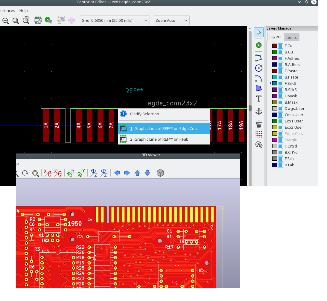
- an edge connector Edit (157.2 KiB, image/png)
#6
AFAIK, pcbnew does not merge edge cuts in footprints with the edge cuts
in the board so a complete board outline is not generated. Someone
please correct me if I'm wrong about this.
Wrong you are WS, Kicad 5.1.4 ;)
See photo for yourself.
Disabling a single layer for putting segment on it is just nonsense.
If a segment of anything must segfault latter , it does matter what tool inserted it.
So, in 2019, manipulating SEGMENT (line) on any layer in footprint editor IS working.
It is working so well that you just have to use a text editor on the source to add one then ctrl-d it as you need.
Next pcbnew is TOTALLY happy with the 5 segments (in my edge connector design) to draw a board.
Conclusion is simple
-this is not a valid limitation
-there is no code to add
-there no new feature here and FE must remove this restriction
(If the polygon tool is not working on this edges cuts layer, the tools have to be disabled for this layer. Not the layer.)
Application: KiCad
Version: 5.1.4, release build
Libraries:
wxWidgets 3.0.2
libcurl/7.37.0 OpenSSL/1.0.2j zlib/1.2.8 libidn/1.28 libssh2/1.4.3
Platform: Linux 4.4.180-102-default x86_64, 64 bit, Little endian, wxGTK
Build Info:
wxWidgets: 3.0.2 (wchar_t,STL containers,
Boost: 1.61.0
OpenCASCADE Community Edition: 6.9.1
Curl: 7.37.0
Compiler: GCC 4.8.5 with C++ ABI 1002
Build settings:
USE_
USE_
KICAD_
KICAD_
KICAD_
KICAD_
KICAD_
KICAD_
BUILD_
KICAD_
KICAD_
KICAD_SPICE=OFF
| Wayne Stambaugh (stambaughw) wrote : | #47 |
I didn't suggest that Edge.Cut segments from footprints were not processed by the gerber plotter. This is why the work around actually works. There is no code in Pcbnew that combines edge cuts from all possible sources into a single geometric entity for things like DRC enclosed polygon checks and 3D model outline rendering. This code needs to be implemented before we allow drawing on the FE edge cut layer. Otherwise, the very next bug reports will be about these issues being broken. Users who use this hack, understand this limitation in Pcbnew.
| Rene Poeschl (poeschlr) wrote : | #48 |
- 00_pr_invest.zip Edit (9.7 KiB, application/zip)
1) I played around with footprints including edge cuts and to me it seems as if drc does combine the lines within a footprint and what is drawn on the board.
2) It also seems to work correctly if two footprints define edge cuts and these are placed right next to each other (such that their edge cuts definition directly combines without an additional line in between them)
3) It also notices if the edge cuts line is not closed within the footprint.
I can then connect the outline ends of this footprint within pcb new and this is then discovered as a closed outline.
---
By the way i am on version 5.1.4.
My test project is attached should anybody be interested (quick and dirty so not all edge cuts lines are orthogonal). It is in the "no drc errors" stage. J2 and J3 together test (2). J2 is modifed to test (3) (It has a broken outline near its top left corner. remove the edge cuts line that closes it to test it.) J1, J2 and J3 together test (1).
So either the DRC algorithm is more advanced than you are aware of or something here happens on accident in the way a user would expect it to work.
| Roger Clark (rogerclarkmelbourne) wrote : | #49 |
Just to add another +1 to this.
I'm currently designing a PCB, where toroid inductors are recessed into the PCB, and I've had to use the trick of making a polyline on another layer, then manually editing the pretty file to move it to the edge cuts layer.
In the past I've also had to manually add cuts under individual components on the PCB after the layout is complete, to provide extra electrical isolation e.g. under opto couplers and also some hall effect sensors, which have 440V on one side and 3.3V on the other.
| Niki Guldbrand (niki-guldbrand-net) wrote : | #50 |
FYI, Kicad has moved to https:/
And if you have a look at issue 1970 in the kicad code tree, you can
see that edge cuts will be available in the upcomming version 6
release.
https:/
Niki
On Sat, 2020-09-19 at 03:19 +0000, Roger Clark wrote:
> Just to add another +1 to this.
>
> I'm currently designing a PCB, where toroid inductors are recessed
> into
> the PCB, and I've had to use the trick of making a polyline on
> another
> layer, then manually editing the pretty file to move it to the edge
> cuts
> layer.
>
> In the past I've also had to manually add cuts under individual
> components on the PCB after the layout is complete, to provide extra
> electrical isolation e.g. under opto couplers and also some hall
> effect
> sensors, which have 440V on one side and 3.3V on the other.
>
| KiCad Janitor (kicad-janitor) wrote : | #51 |
KiCad bug tracker has moved to Gitlab. This report is now available here: https:/
| Changed in kicad: | |
| status: | In Progress → Expired |
On Thu, Nov 14, 2013 at 07:24:07PM -0000, Stephen Pflanze wrote:
> In the Module Editor I need to be able to put a graphic line in the
> Edge.Cuts layer just as can be done in the PCB editor.
Currently that's not possible due to some limitation in the DRC code,
IIRC. Could be possibly be fixed, stay tuned.
--
Lorenzo Marcantonio
Logos Srl