
© 2004
Canonical Ltd.
•
Terms of use
•
Data privacy
•
Contact Launchpad Support
•
Blog
•
Careers
•
System status
•
0e1f616
(Get the code!)
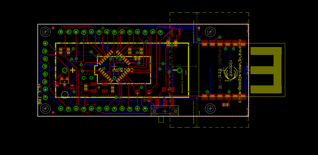
I'm talking about document as in an additional graphical layer (just like pcbnew where there is document layer) where you draw additional graphical information or have text. In eagle there are two document layers (front and back of board) for components is an additional drawing layer that does not get printed for fabrication, but is available for design time and documentation, i.e. print out the for design documentation.
For example I've used it in the past to document the component clearances around RF modules that have integrated antennas of where I can have traces, so I have my silkscreen outline of the footprint as per normal, I also have an additional outline around the footprint that don't show up in fabrication output, this shows me where not to place components and where I need to place it against a board edge, so is very useful for visually indicating where I can run tracks and place other components or anything else I need at design time..
Another example is a connector that hang over the edge of the board, the silkscreen is only useful for the actual board, but the document layer can have the rest of the outline to give you an idea of the full component dimensions. When panellising, these overhangs need to be taken into account as they interfere with neighbour panel, or may overlap another panel, but you don't want the silkscreen on the other panel.
Also for better documenting the component outlines that complement silkscreen, from the examples below you can see full component outlines that don't interfere with pads.
A couple of examples attached