
© 2004
Canonical Ltd.
•
Terms of use
•
Data privacy
•
Contact Launchpad Support
•
Blog
•
Careers
•
System status
•
a60fb26
(Get the code!)
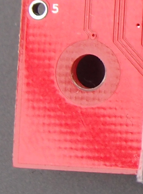
> Did you look at this picture and think everything should look the same, the copper, the pcb, etc?
Yes because as I explained in the previous post I assumed / implemented the copper as not plated.
As I said that I agree, the plated copper will not look like raw copper, it will look as plated, but it was not implemented.
Maybe someone?! can implement the plated copper so it will look as you suggest.
> This patterning should be removed from everything but the actual exposed by soldermask opening area.
> The liquid soldermask pours over the pattern and covers it up.
> The solder paste mask will also cover up any pattern from anything.
I implemented the soldermaks pattern as I see it on the PCBs I am used (see attached an example)
It may be possible there are other PCBs types that I am not used or I dont know.
So the other types may need implementation.
There is already one option to enable/disable textures patterns that you can use.
I don't have time now to implement other options,
but feel free to implement other scenarios!