3D Viewer: Better raytracing textures for copper layers

Bug #1680527 reported by Andrey Kuznetsov
8
This bug affects 1 person
Affects Status Importance Assigned to Milestone
KiCad
Fix Released
Unknown

Bug Description

http://i.imgur.com/jleDkjH.png

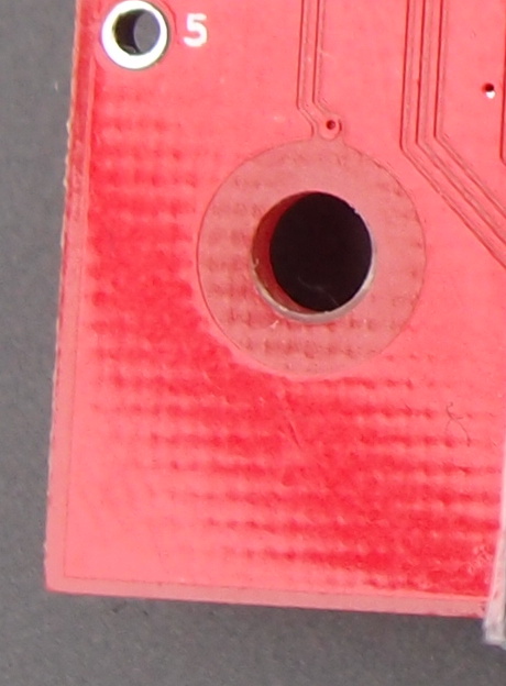
What does Raytracing procedural textures for exactly? If it's to simulate the fiber board, it's done incorrectly:
1. the pattern is too coarse
2. the pattern is applied to copper, which should not happen if the pattern is meant to enhance the texture of the PCB

Application: kicad
Version: (2017-04-05 revision bf21640ae)-makepkg, release build
Libraries: wxWidgets 3.0.2
           libcurl/7.52.1 OpenSSL/1.0.2k zlib/1.2.11 libssh2/1.8.0 nghttp2/1.19.0 librtmp/2.3
Platform: Windows 8 (build 9200), 64-bit edition, 64 bit, Little endian, wxMSW
- Build Info -
wxWidgets: 3.0.2 (wchar_t,wx containers,compatible with 2.8)
Boost: 1.60.0
Curl: 7.52.1
KiCad - Compiler: GCC 6.3.0 with C++ ABI 1010
        Settings: USE_WX_GRAPHICS_CONTEXT=OFF
                  USE_WX_OVERLAY=OFF
                  KICAD_SCRIPTING=ON
                  KICAD_SCRIPTING_MODULES=ON
                  KICAD_SCRIPTING_WXPYTHON=ON
                  KICAD_SCRIPTING_ACTION_MENU=OFF
                  BUILD_GITHUB_PLUGIN=ON
                  KICAD_USE_OCE=ON

Tags: 3d-viewer
tags: added: 3d-viewer
Revision history for this message
Mario Luzeiro (mrluzeiro) wrote :

> 1. the pattern is too coarse

It is OK to edit the source code and propose/submit a new values for the pattern.
Or maybe add an option so users can change this parameters.

When I developed that texture I based my tunning on real PCB photos. Also it looks similar to other CAD tools, eg:
http://www.sasabremec.com/wp-content/uploads/Untitled1.png

> 2. the pattern is applied to copper, which should not happen if the pattern is meant to enhance the texture of the PCB

You are right in a real PCB that pattern comes from the FR4 substrate and not from the copper. As the copper is compressed against the substrate it will get also some degree of that "ondulation" (modulated to the pattern of the substrate).

In the 3D-Viewer implementation is not possible to simulate the mechanical / physical adaption of the copper to the substrate.
So the way I implemented was to create the parent texture for the substrate and then the copper texture is a soften derived from that parent, then the Solder mask again is a soft derivation from copper texture. (as again in real life the liquid mask will adapt and get smooth to the surface it is deposited)

These factors are also possible to be changed on the source code.

Revision history for this message
Andrey Kuznetsov (kandrey89) wrote :

Yes, Altium does it too but it looks much better and they do not apply it to copper. I don't believe that applying the texture to copper is correct, from every PCB I've looked at, I do not see fiber board textured impression in the exposed copper pour, either way even if there is a tiny texture in the copper <5% of original, what should be shown to the user is a plated copper pad, ENIG, ENEPIG, HASL, etc and those definitely would not have that texture.
http://i.imgur.com/zNo1y65.png
http://i.imgur.com/QYkp3oW.png

Revision history for this message
Mario Luzeiro (mrluzeiro) wrote :

I agree that the plated copper should look different.
When I implemented it I didn't thought about the plated copper but only on raw copper.

But the copper suffers from the board texture. That is why you see the texture on the "green" solder mask (it has some transparency). That is in fact some of the copper texturing and some of texture of the solder mask (more smooth)

When the copper is plated, it will level the copper and we see the plated finish material.

Revision history for this message
Andrey Kuznetsov (kandrey89) wrote :

Did you look at this picture and think everything should look the same, the copper, the pcb, etc?
https://s-media-cache-ak0.pinimg.com/originals/1f/8c/a1/1f8ca1e108fb9513c283ac32e6c0215f.jpg

1. the soldermask gets rid of the fiber pattern see: http://kingofwallpapers.com/pcb/pcb-005.jpg
2. The majority of the PCBs are made such that the copper shows no PCB patterning see: https://stab-iitb.org/electronics-club/assets/using-eagle-to-design-pcbs/image03.jpg

This patterning should be removed from everything but the actual exposed by soldermask opening area.
The liquid soldermask pours over the pattern and covers it up. The copper from all the PCBs that I've seen either has a VERY VERY TINY patern to it or no discernable pattern at all. Gold, tin, or other process plating gets rid of the pattern completely! The solder paste mask will also cover up any pattern from anything.

Revision history for this message
Mario Luzeiro (mrluzeiro) wrote :

> Did you look at this picture and think everything should look the same, the copper, the pcb, etc?

Yes because as I explained in the previous post I assumed / implemented the copper as not plated.
As I said that I agree, the plated copper will not look like raw copper, it will look as plated, but it was not implemented.

Maybe someone?! can implement the plated copper so it will look as you suggest.

> This patterning should be removed from everything but the actual exposed by soldermask opening area.
> The liquid soldermask pours over the pattern and covers it up.
> The solder paste mask will also cover up any pattern from anything.

I implemented the soldermaks pattern as I see it on the PCBs I am used (see attached an example)
It may be possible there are other PCBs types that I am not used or I dont know.
So the other types may need implementation.

There is already one option to enable/disable textures patterns that you can use.

I don't have time now to implement other options,
but feel free to implement other scenarios!

Jeff Young (jeyjey)
Changed in kicad:
importance: Undecided → Wishlist
status: New → Triaged
Jeff Young (jeyjey)
summary: - 3D Viewer: Raytracing Procedural Textures
+ 3D Viewer: Better raytracing textures for copper layers
Revision history for this message
KiCad Janitor (kicad-janitor) wrote :

KiCad bug tracker has moved to Gitlab. This report is now available here: https://gitlab.com/kicad/code/kicad/-/issues/2058

Changed in kicad:
status: Triaged → Expired
Changed in kicad:
importance: Wishlist → Unknown
status: Expired → Fix Released
To post a comment you must log in.
This report contains Public information  
Everyone can see this information.

Other bug subscribers

Remote bug watches

Bug watches keep track of this bug in other bug trackers.