Connectivity algorithm failure

Bug #1787961 reported by Franck78
6
This bug affects 1 person
Affects Status Importance Assigned to Milestone
KiCad
Fix Released
High
Seth Hillbrand

Bug Description

Hello,

Short version, place three pads, duplicate one, make two tracks. Apparently identical pieces but not same reaction to edit.

Open the attachment

-launch pcbnew
-load some design
-edit->global-deletion->clearboard
(the netlist is still active and maybe it's a feature)
Add some footprints this way (select a basic single test point pad)

-o place it
-ctrl-D the pad, place it
-link the two pads with a track
-o place it
-o place it
-again, link the two pads

-e on track1, assign a net from the dropdown list, validate
-e on track2, assign a net from the dropdown list, validate

One track accept and memorize the edit.
The other track, no.
From a user's point of view. It's to same tracks no reacting the same.

-reload netlist (not the design)
-pose the mesh somewhere
-now, no more assignment of net names for either track

-o
-o
-link the two pads, again
-e, choose net name
and net name change is accepted.

Application: kicad
Version: 5.0.0, release build
Libraries:
    wxWidgets 3.0.2
    libcurl/7.37.0 OpenSSL/1.0.2j zlib/1.2.8 libidn/1.28 libssh2/1.4.3
Platform: Linux 4.4.143-65-default x86_64, 64 bit, Little endian, wxGTK
Build Info:
    wxWidgets: 3.0.2 (wchar_t,STL containers,compatible with 2.8) GTK+ 2.24
    Boost: 1.61.0
    OpenCASCADE Community Edition: 6.9.1
    Curl: 7.37.0
    Compiler: GCC 4.8.5 with C++ ABI 1002

Build settings:
    USE_WX_GRAPHICS_CONTEXT=OFF
    USE_WX_OVERLAY=OFF
    KICAD_SCRIPTING=ON
    KICAD_SCRIPTING_MODULES=ON
    KICAD_SCRIPTING_WXPYTHON=ON
    KICAD_SCRIPTING_ACTION_MENU=ON
    BUILD_GITHUB_PLUGIN=ON
    KICAD_USE_OCE=ON
    KICAD_USE_OCC=OFF
    KICAD_SPICE=OFF

Tags: pcbnew
Revision history for this message
Franck78 (fbourdonnec) wrote :
Jeff Young (jeyjey)
Changed in kicad:
status: New → Confirmed
importance: Undecided → High
milestone: none → 5.1.0
assignee: nobody → Jeff Young (jeyjey)
Revision history for this message
Jeff Young (jeyjey) wrote :

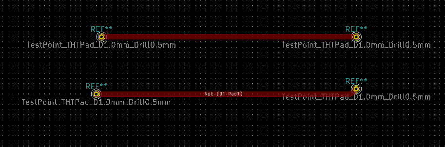
The Track & Via Properties dialog only updates the selected nets. Commit() then propagates the nets to connected items. In one case Commit() propagates from the pad out, and so clears the net.

In the other case, Commit() doesn't propagate because when it rebuilds the clusters the pad's CN_ITEM doesn't have the track in its connected items list and so the track ends up in a different cluster.

Because the second case isn't propagated, you can even end up with different segments of the track being assigned different nets.

Revision history for this message
Jeff Young (jeyjey) wrote :

I was going to post my simple test board, but of course saving and re-opening it fixes it.

I can fix Track & Via Properties to chain the tracks & pads when assigning a Net, but this problem with the Connectivity Algorithm bothers me a lot more.

Revision history for this message
Jeff Young (jeyjey) wrote :

@Seth, could you give this a look? I'm lost in the Connectivity/RTree stuff.

I went ahead and attached my simple board so you could see what you need to create to trigger it. Note however that you have to create it from scratch; the simple board when opened does NOT exhibit the bug.

Revision history for this message
Seth Hillbrand (sethh) wrote :

Sure. My thought would be three steps:

1) Disallow assigning nets to tracks as this is confusing and always overwritten
2) Remove the net from tracks that are not connected to a pad
3) Allow net 0 (unassigned) tracks to connect to any pad and thereby acquire its net

Do any of these steps seem improper? It changes how users would work with unconnected tracks, but I feel that this might provide a smoother workflow and by more internally consistent.

Thoughts?

Revision history for this message
Jeff Young (jeyjey) wrote :

@Seth, sorry, I wasn't specific enough. I was going to handle the original bug report stuff. I was just hoping you could look at the possible Connectivity Algorithm bug I discovered in comment #2 (which funnily enough is why one of the cases actually works today).

Revision history for this message
Jeff Young (jeyjey) wrote :

As for Seth's specific comments, (3) was already done for 5.0.

I was going to go the other way with (1). If you do change the net of a selected track segment, I think it's clear enough that you want to change the net of all connected items.

This comes up often when you layout a board from scratch (ie: not from a schematic).

Revision history for this message
Franck78 (fbourdonnec) wrote :

I would be happy to understand why the duplicate footprint creates that diff OR the shortest sequence of event to produce the bug if the ctrl-D have nothing to do.

-my first reaction was, in fact, why a netlist still exists after edit->clearboard ?

Revision history for this message
Seth Hillbrand (sethh) wrote :

@Jeff-

Oh, no worries. Yes, I'll look at the CN_ITEM business and leave you the heavy lifting :)

On (1), I worry that the solution you are proposing will open a can of worms as it potentially breaks the netlist by changing a pad's net. I think (warning, opinion here) it also leads to confusion of the kind we've been seeing recently about the differences between tracks and nets. I'd prefer if we were more explicit in our expectations of where nets come from (pads and zones)

Revision history for this message
Jeff Young (jeyjey) wrote :

@Seth, I merged a compromise version which tells the user the pads' nets will be changed and gives them the opportunity to cancel. Let me know what you think of it.

(The connectivity bug remains outstanding.)

summary: - failure to assign net
+ Connectivity algorithm failure
Changed in kicad:
assignee: Jeff Young (jeyjey) → nobody
Revision history for this message
Seth Hillbrand (sethh) wrote :

OK I'll take a look at the conn bug.

On the pad/net change thing, I think we need a wider question to the list. I'm extremely uneasy with this changing, at least without full back annotation in place but I'd prefer we pose the question to the list as I may be overthinking this or there may be deeper concerns that we need to address.

Changed in kicad:
assignee: nobody → Seth Hillbrand (sethh)
Revision history for this message
Seth Hillbrand (sethh) wrote :

@Jeff- Are you still able to trigger this bug? I'm not having luck anymore and I think it might have been addressed with some of the other changes.

Revision history for this message
Jeff Young (jeyjey) wrote :

@Seth, it still reproduces for me.

Open the board I attached in #4.
Delete all 4 pads and two tracks.
Select footprint tool and add a SolderWirePad_single_0-8mmDrill.
Duplicate the footprint.
Select the track tool and connect the two footprints.
Select footprint tool and add two more SolderWirePad_single_0-8mmDrill.
Select the track tool and connect the two new ones.
Select the first track; properties; change the net to diff-.
You should get a dialog asking you if you want to update the pad. That's good, but only one pad gets updated.
Select the second track; properties; change the net to diff-.
No dialog; neither pad's net is updated.

Revision history for this message
Tomasz Wlostowski (twlostow) wrote :

@Jeff, @Seth, putting the bug on hold, we need to discuss how to proceed PM first.

Changed in kicad:
status: Confirmed → Incomplete
Revision history for this message
Wayne Stambaugh (stambaughw) wrote :

@Tom, what is it that I need to decide here before we proceed?

Revision history for this message
Seth Hillbrand (sethh) wrote :

@Wayne/Tom - Ping. Here or e-mail. I'd like to fix or close

Revision history for this message
Tomasz Wlostowski (twlostow) wrote :

@Seth/Wayne: the 'bug' shows up because of the pad net update code by Jeff (in the track/via properties dialog, bool DIALOG_TRACK_VIA_PROPERTIES::TransferDataFromWindow()). IMHO the only way pads could have their net changed is by editing the netlist/schematic or directly in the pad properties window (and only there).

I would just disable the pad update feature and close this bug report.

Revision history for this message
Wayne Stambaugh (stambaughw) wrote :

@Tom, do you mean disable the track net change feature in the track properties dialog or the pad net change feature in the pad properties dialog or both? In either case, allowing users to change nets in the board editor is dangerous because the next time they update the net list from the schematic, their changes will get clobbered. I agree that this this should be disabled until we implement some type of back annotation feature that allows net (and other) changes in the board editor to propagate back to the schematic editor. Anyone else opposed to this?

Revision history for this message
Tomasz Wlostowski (twlostow) wrote :

@Wayne, I mean neither of the above (I'm ok with selecting a net for a track/via/pad in the respective dialogs), I meant the code in dialog_track_via_properties.cpp (lines 343 onwards):

for( auto& item : m_items )
 {
            auto boardItem = static_cast<BOARD_CONNECTED_ITEM*>( item );
            connectivity->GetConnectedPads( boardItem, &connectedPads );
        }

        for( D_PAD* pad : connectedPads )
        {
            if( pad->GetNetCode() != newNetCode )
                changingPads.push_back( pad );
}

....

It propagates the new (changed) net of a track edited through the Track/Via properties dialog to all pads connected to that track. Kicad asks if the user wants these pads nets to be changed, but IMHO it's still dangerous and just not the way proper PCB designs are made (there are people who want to draw PCBs without drawing a schematic/having a netlist, but should we cater for such exotic needs?). It also triggers a hidden bug in the connectivity algorithm which this report is about, but it wouldn't have surfaced otherwise.

Tom

Revision history for this message
Jeff Young (jeyjey) wrote :

Yes, I'm definitely opposed. We can't have a Net control in the Edit Track & Via properties that is ignored when you click OK. (The control is not new; it's been there at least since 4.0.)

The control is also useful. Our current board update mechanism doesn't always update tracks. So if you change (for instance) a global label in your schematic and then update the board, you'll have tracks that still refer to the old net. If we remove the feature then it's unclear how you'd fix that. (I'm sure there's some way to kick the connectivity algorithm to get the pads propagated outwards, but this certainly isn't obvious to a user.)

But I also disagree with the fundamental notion that the error is caused by the change. The error appears *before* the new code is run. The new code only *exposes* the error, it doesn't cause it.

Revision history for this message
Tomasz Wlostowski (twlostow) wrote :

@Jeff I'm going to fix the connectivity algo issue anyway, but I don't understand how global labels (on the schematic) are related to wrongly updated nets on the PCB. It looks like another bug to me. Do you have any project where this could be easily reproduced?

Tom

Revision history for this message
Jeff Young (jeyjey) wrote :

@Tom, cool, I'll feel much better with the bug fixed, no matter what we do with the other stuff.

I've attached a project. If you open the schematic and change one of the transformer secondary windings at the left of the lower half (say, from 48VAC_1 to 52VAC_1) and then update the PCB, the tracks won't get updated. (They're the 4 short stubby ones on the front at the top right and bottom right of the board.)

Revision history for this message
Tomasz Wlostowski (twlostow) wrote :

@Jeff, @Seth, @Wayne: Done. The bug actually wasn't in the connectivity algorithm, but spread over several other places...

Revision history for this message
Seth Hillbrand (sethh) wrote :

Thanks Tom!

Changed in kicad:
status: Incomplete → Fix Committed
Revision history for this message
Franck78 (fbourdonnec) wrote :

Ah good news, a weird bug ;)

I have another one, classified as wish but really is a bug and only the author of the router can fix.

#1789009

Thank you
Franck

Revision history for this message
Wayne Stambaugh (stambaughw) wrote :

@Tom, thanks for fixing this!

Changed in kicad:
status: Fix Committed → Fix Released
To post a comment you must log in.
This report contains Public information  
Everyone can see this information.

Other bug subscribers

Remote bug watches

Bug watches keep track of this bug in other bug trackers.