Differential pairs use DP spacing when checking clearance to component pads

Bug #1787275 reported by Andrew Zonenberg
10
This bug affects 2 people
Affects Status Importance Assigned to Milestone
KiCad
Fix Released
Medium
Jeff Young

Bug Description

Test file:

https://github.com/azonenberg/starshipraider/blob/6062a876ba20484db9cd9ebcb7b82e7b629feb55/boards/iob-characterization-v02/iob-characterization-v02.kicad_pcb

Steps to reproduce:

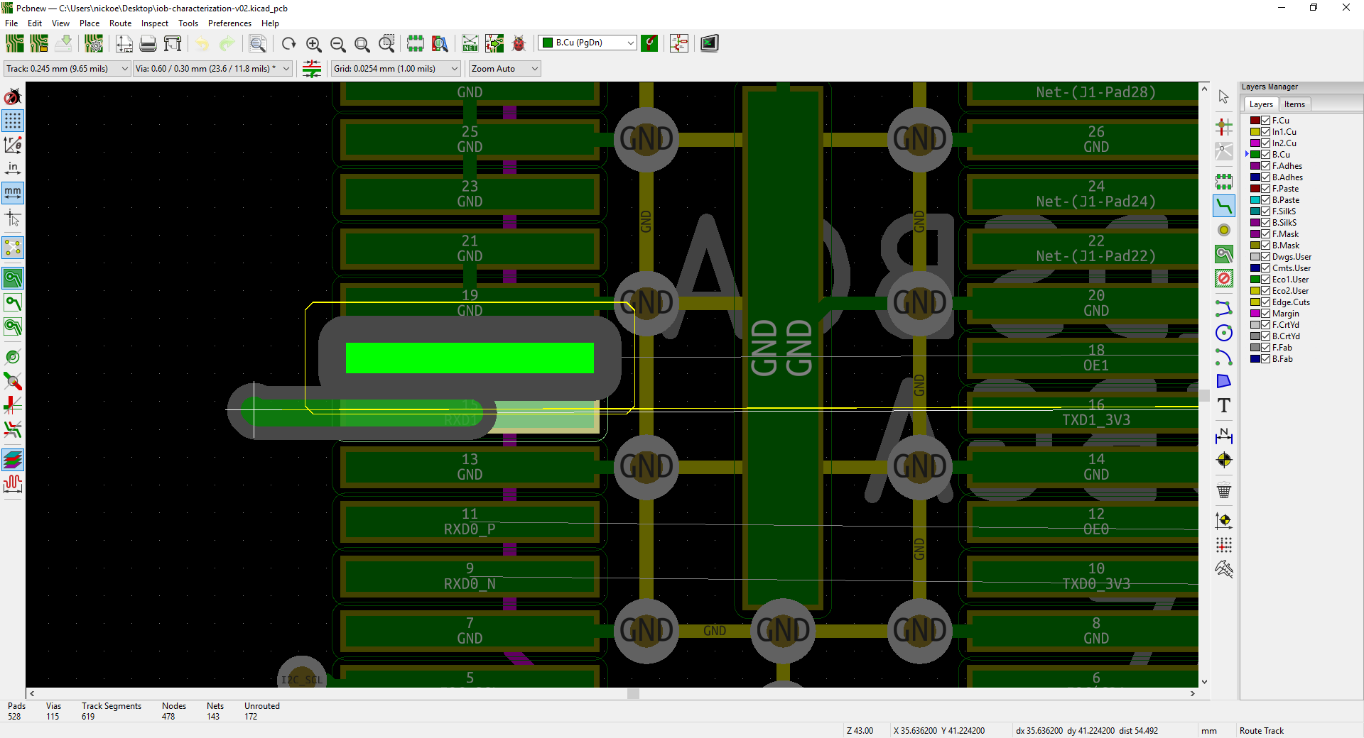
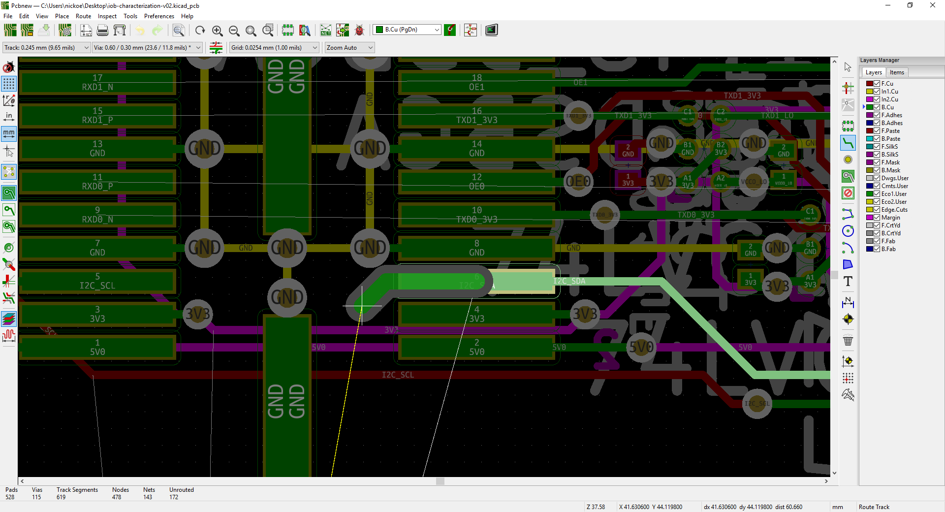
Try to draw an 0.245mm wide trace from the RX0/1 P/N pairs on the large connector at the left side of the board.

Expected result: 0.245mm trace with 0.125mm clearance can be drawn off an 0.5mm pitch connector

Actual result: DRC errors, trace cannot be drawn. In "highlight collisions" mode, the collision box around the connector pad is significantly larger than it should be.

Workaround: Switch to "highlight collisions" mode and "allow DRC errors". Draw a short stub trace off the pad, then switch to "shove" mode to draw another trace segment. The rest of the trace can be routed fine after this.

KiCAD info:

Application: kicad
Version: (6.0.0-rc1-dev-316-ga88831d7a), release build
Libraries:
    wxWidgets 3.0.2
    libcurl/7.52.1 OpenSSL/1.0.2l zlib/1.2.8 libidn2/0.16 libpsl/0.17.0 (+libidn2/0.16) libssh2/1.7.0 nghttp2/1.18.1 librtmp/2.3
Platform: Linux 4.9.0-6-amd64 x86_64, 64 bit, Little endian, wxGTK
Build Info:
    wxWidgets: 3.0.2 (wchar_t,wx containers,compatible with 2.8) GTK+ 2.24
    Boost: 1.62.0
    Curl: 7.52.1
    Compiler: GCC 6.3.0 with C++ ABI 1010

Build settings:
    USE_WX_GRAPHICS_CONTEXT=OFF
    USE_WX_OVERLAY=OFF
    KICAD_SCRIPTING=OFF
    KICAD_SCRIPTING_MODULES=OFF
    KICAD_SCRIPTING_WXPYTHON=OFF
    KICAD_SCRIPTING_ACTION_MENU=OFF
    BUILD_GITHUB_PLUGIN=ON
    KICAD_USE_OCE=OFF
    KICAD_USE_OCC=OFF
    KICAD_SPICE=OFF

Tags: pcbnew pns
Changed in kicad:
status: New → Confirmed
milestone: none → 5.1.0
tags: added: pcbnew
Revision history for this message
Nick Østergaard (nickoe) wrote :

This looks really strange I can reproduce it on windows. It is of course important that you select the track width as specified in the bug description.

It happens with pin 9, 11, 15, and 17 on J1.

Application: pcbnew
Version: (6.0.0-rc1-dev-314-g8fd686e8f), release build
Libraries:
    wxWidgets 3.0.3
    libcurl/7.54.1 OpenSSL/1.0.2l zlib/1.2.11 libssh2/1.8.0 nghttp2/1.23.1 librtmp/2.3
Platform: Windows 8 (build 9200), 64-bit edition, 64 bit, Little endian, wxMSW
Build Info:
    wxWidgets: 3.0.3 (wchar_t,wx containers,compatible with 2.8)
    Boost: 1.60.0
    OpenCASCADE Community Edition: 6.8.0
    Curl: 7.54.1
    Compiler: GCC 7.1.0 with C++ ABI 1011

Build settings:
    USE_WX_GRAPHICS_CONTEXT=OFF
    USE_WX_OVERLAY=OFF
    KICAD_SCRIPTING=ON
    KICAD_SCRIPTING_MODULES=ON
    KICAD_SCRIPTING_WXPYTHON=ON
    KICAD_SCRIPTING_ACTION_MENU=ON
    BUILD_GITHUB_PLUGIN=ON
    KICAD_USE_OCE=ON
    KICAD_USE_OCC=OFF
    KICAD_SPICE=ON

Revision history for this message
Nick Østergaard (nickoe) wrote :
Revision history for this message
Nick Østergaard (nickoe) wrote :
Changed in kicad:
importance: Undecided → Medium
Revision history for this message
Nick Østergaard (nickoe) wrote :

Git bisect gave me this:

44c1f5785be0ee7a9238c9754ac4909d2748aeb6 is the first bad commit
commit 44c1f5785be0ee7a9238c9754ac4909d2748aeb6
Author: Seth Hillbrand
Date: Sun Jun 17 16:31:00 2018 -0700

    pcbnew: Set dp clearance based on netclass

    Minimum differential pair clearance should be limited to the netclass
    differential pair spacing. This also cleans up some unused code that
    was left over from previous work on differential pair clearances.

    Fixes: lp:1673632
    * https://bugs.launchpad.net/kicad/+bug/1673632

:040000 040000 765f0d9de771a838254b4fb940443c5490fdb12a ddffb1608f107fa5f2b5425df4844f458dba2f8e M pcbnew

Revision history for this message
Andrew Zonenberg (azonenberg) wrote :

The commit linked above is wrong. Differential pair spacing is the minimum space from that trace to the other leg of the differential pair. In some cases (connectors especially) it might be necessary to have the clearance to *other* nets be significantly smaller.

In general I'd say that the netclass copper clearance should be used for diffpair clearance.

Revision history for this message
Seth Hillbrand (sethh) wrote :

This is an issue with single net routing to a differential pair. Diff pair gap in the board is set to 0.25mm, which cannot be achieved with 0.5mm pitch. But we should be using the differential pair gap when routing a single trace.

Changed in kicad:
assignee: nobody → Seth Hillbrand (sethh)
Revision history for this message
Andrew Zonenberg (azonenberg) wrote :

In fact I would even say the pair spacing should not be considered a hard clearance limit. Trivial example: a loosely coupled pair of traces with 0.7mm spacing being routed into an 0.5mm connector or IC needs to get pushed to a tighter spacing at the end, then fan out to 0.7mm spacing as soon as practical. It shouldn't fail DRC because the connector is less than 0.7mm pitch, as long as the actual DRC clearance limit (say 0.125 mm) is respected.

Revision history for this message
Andrew Zonenberg (azonenberg) wrote :

Also, 0.245mm traces at 0.25mm spacing *does* fit in 0.5mm pitch. However, the connector pads are wider than 0.245mm so you get a false DRC error.

Try routing this trace differentially, that doesn't work either. Because, even though the trace works, Samtec's recommended pad is too wide to have 0.25mm clearance.

Maybe the fix should be to ignore pad-to-pad clearance in the diffpair DRC calculation? It looks like the problem is that the DRC is trying to provide 0.25mm of clearance from pad 13 to pad 11, rather than only from pad 13 to the newly drawn trace.

Revision history for this message
Seth Hillbrand (sethh) wrote :

You are correct, the spacing can fit in the pitch.

However, this is not DRC. The board does not fail a DRC check. The differential pair spacing is there to allow differential pair routing at a specific distance. If the pads are too close together, then that means the design rules are wrong or the pads are wrong. In the future we will have more configurable design rules but for now, we shouldn't make a bunch of special cases to address individual configurations as this as it will lead to more problems.

summary: - P&S router gives false positive DRC errors
+ Routing single track in differential pair uses dp clearance
Revision history for this message
Andrew Zonenberg (azonenberg) wrote : Re: Routing single track in differential pair uses dp clearance

What about if you need to route a diffpair through a tight space (say, a BGA via field)? It's very possible to have a different net (i.e. not part of the diffpair) be less than one pair spacing away from one leg. Coupling shouldn't be a serious problem as long as it doesn't parallel for a large portion of the run.

The spacing rule as it stands makes routing diffpairs impossible in any remotely congested area of a board.

Revision history for this message
Seth Hillbrand (sethh) wrote :

That is correct. We do not currently support area-based clearance rules. That is planned for the future.

Revision history for this message
Andrew Zonenberg (azonenberg) wrote :

I'm not asking for area-based clearance or anything complex. I'm asking for a very simple conditional when doing clearance checks on a track:

1) Minimum clearance from a DP leg to a *track* for the other DP leg is the netclass DP spacing
2) Minimum clearance from a DP leg to a *pad* for the other DP leg is the netclass track clearance
3) Minimum clearance from a DP leg to *any track or pad not part of the DP* is the netclass track clearance

Is this difficult to implement? Do you believe any of these rules are incorrect behavior? (And if so, how much high-speed digital layout experience do you have to based your claim on?)

For example, in my example board the DP legs should be kept 250 um apart from each other, however it should be legal for one leg to get within 125 um of a connector pad for the other DP leg, or 125 um of any other track. Later on we can add more advanced design rules to limit this incidental contact to prevent excessive coupling to non-DP tracks, but for the moment I believe it's important for the router to err on the side of being permissive rather than prohibitive.

It's a lot easier to manually re-route a few tracks to ensure sufficient clearance for EMC reasons, than to change design rules or do other awkward things because KiCAD refuses to let you escape a BGA, connector, etc.

summary: - Routing single track in differential pair uses dp clearance
+ Differential pairs use DP spacing when checking clearance to non-coupled
+ nets
Revision history for this message
Seth Hillbrand (sethh) wrote : Re: Differential pairs use DP spacing when checking clearance to non-coupled nets

I'll split this off into two issues. The one I was originally addressing was the single-track routing. I'll track that issue over at lp: 1787766

We can look at adding the conditionals you describe separately.

Changed in kicad:
assignee: Seth Hillbrand (sethh) → nobody
importance: Medium → Wishlist
milestone: 5.1.0 → none
status: Confirmed → New
Revision history for this message
Andrew Zonenberg (azonenberg) wrote :

This should be much higher than "wishlist" severity. This is a major regression, boards that were routable prior to 44c1f5785be0ee7a9238c9754ac4909d2748aeb6 no longer work.

If you don't want to deal with it now, maybe we should roll back that commit until a long-term fix is available?

Revision history for this message
Lain (lainpants) wrote :

To me, this is incorrect behavior on the part of the router. The netclass clearance defines the required spacing between either leg of the differential pair and other nets in the design, while the differential pair spacing defines *only* the spacing between the legs of a single diffpair (the coupled nets).

As someone trying to move to kicad who also lays out high-density boards with many diffpairs, this bug is a serious impediment.

Perhaps the most salient point, however, is that the router used to behave as expected, but now does not.

Revision history for this message
Seth Hillbrand (sethh) wrote :

OK, perhaps I am misunderstanding the report.

The original bug, I read as trying to route a single, non-dp trace on a dp-labeled pair. That is broken as the clearance used is currently the dp spacing rather than the single track clearance. We are addressing that separately.

It sounds like Andrew is saying that the clearance between a dp leg and another trace that is not the dp is _also_ using the dp clearance. If my understanding of that is correct, then I cannot reproduce this issue. I've tried with the board linked to this report. See attached picture. Here all tracks are dragged within their minimum clearances to each other. The RXD0_P and GND are 0.125mm away while RXD0_P and RXD0_N are 0.25mm. This seems consistent with the design rules on the board.

If a user wants to route differential traces with varying gaps, you can set the dp gap smaller in the design rules and override them while routing (right-click, differential pair settings).

If there's a bug here, let's clarify the single, specific bug.

Revision history for this message
Andrew Zonenberg (azonenberg) wrote :

So, after a bit of digging it seems I slightly misunderstood what was causing the original issue.

In differential pair mode, the clearance check is failing on the leg-to-leg connector pads (not the legs to the adjacent non-pair pads) since they're less than 0.25 mm apart.

The fix for this issue is to ensure that the DP clearance is only imposed from trace to trace, and the normal netclass clearance is used for trace-to-pad checks. In the screenshot, it should be legal for pad 15 to be less than 0.25mm from pad 17 as long as the traces fan out to the correct distance once they leave the pads.

summary: - Differential pairs use DP spacing when checking clearance to non-coupled
- nets
+ Differential pairs use DP spacing when checking clearance to component
+ pads
Revision history for this message
Wayne Stambaugh (stambaughw) wrote :

I believe this bug was fixed recently.

Revision history for this message
Jeff Young (jeyjey) wrote :

Yes, fixed as a side-effect of https://bugs.launchpad.net/kicad/+bug/1789690.

Changed in kicad:
status: New → Fix Committed
importance: Wishlist → Medium
assignee: nobody → Jeff Young (jeyjey)
milestone: none → 5.1.0
Changed in kicad:
status: Fix Committed → Fix Released
To post a comment you must log in.
This report contains Public information  
Everyone can see this information.

Other bug subscribers

Remote bug watches

Bug watches keep track of this bug in other bug trackers.