Show net names of copper zones - Wishlist
| Affects | Status | Importance | Assigned to | Milestone | |
|---|---|---|---|---|---|
| KiCad |
New
|
Unknown
|
|||
Bug Description
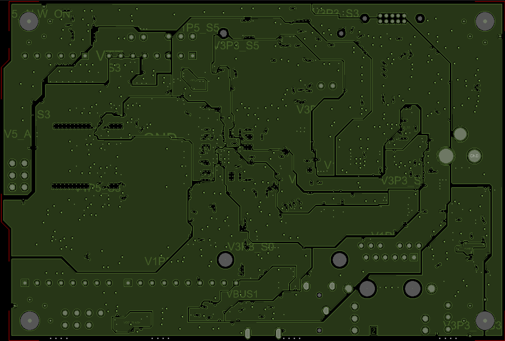
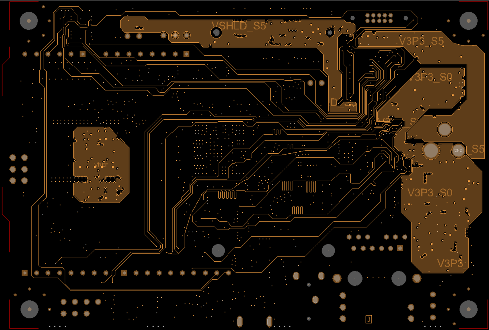
This is a wishlist feature. Especially on 4-layer+ boards, many layers have be completely a ground plane or a power plane. Some layers may be used for power distribution, and have a 5V zone in one area, a 3.3V zone in another area, 1.8V in another area, etc.
What would be handy, when initially laying down the zones or during a review, is to quickly see the net connection of the zones while also seeing the entire board. Typically, when fully zoomed out the net names on tracks cannot be seen so the net connectivity of zones cannot be determined.
I'm proposing that net name text is shown inside the zone outline, similar to how it's shown on tracks. The text size should scale along with the zoom level, so the text is large enough to read easily regardless of the viewport (of course the text shouldn't grow outside the zone boundary). Also, for large zones it may make sense to show the net name text in a few different places (on some type of grid) so the eye doesn't need to hunt around for the text on any given zone; this is most important if the zone is snake-list instead of a large block.
I'll provide two examples of what this could look like, though admittedly the text is often clipped here so a better implementation may be possible.
Being able to select a highlight color for nets would also help with this.

| Changed in kicad: | |
| importance: | Undecided → Wishlist |
| tags: | added: pcbnew |
| Changed in kicad: | |
| status: | New → Triaged |
| Changed in kicad: | |
| importance: | Wishlist → Unknown |
| status: | Expired → New |
Note: there's an interesting idea in the linked duplicate.