
© 2004
Canonical Ltd.
•
Terms of use
•
Data privacy
•
Contact Launchpad Support
•
Blog
•
Careers
•
System status
•
1b1ed1a
(Get the code!)
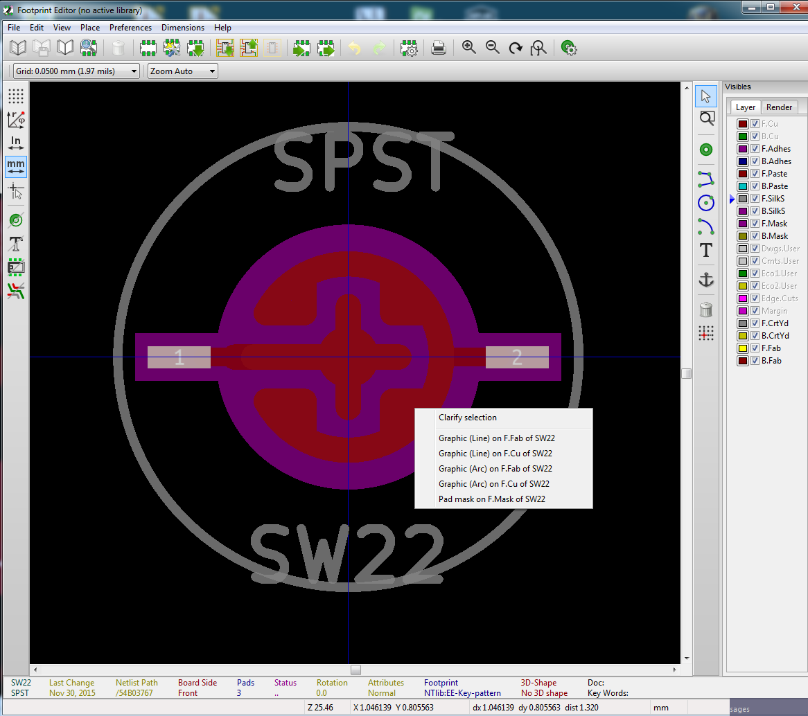
@Wiz, thanks for the input. How did you do it? I tried to add a pin in Footprint Editor, and unticked Layers affacted (eg.
one pin for Copper= F.Cu only,
other pin for Copper B.Cu,
next pin is SMD Copper=none, and F.Mask on etc.
It is a bit tricky but workable way of creating different shape layers for a single pin.
May have a "default size pads on layers" checkbox (default on), and if unticked, tabular format should be better.
One more thing I have already done: creating complex shapes (e.g. on F.Cu) by drawing Graphics Lines, and move graphics lines to F.Cu layer. (see attached picture of the carbon paste keyboard connector image)
Now it seems this function is not "very far" from being workable..maybe worth working on it as it would be a huge advance!!