Zone vs. Soldermask clearance collisions at corners
| Affects | Status | Importance | Assigned to | Milestone | |
|---|---|---|---|---|---|
| KiCad |
Fix Committed
|
Medium
|
Jeff Young | ||
Bug Description
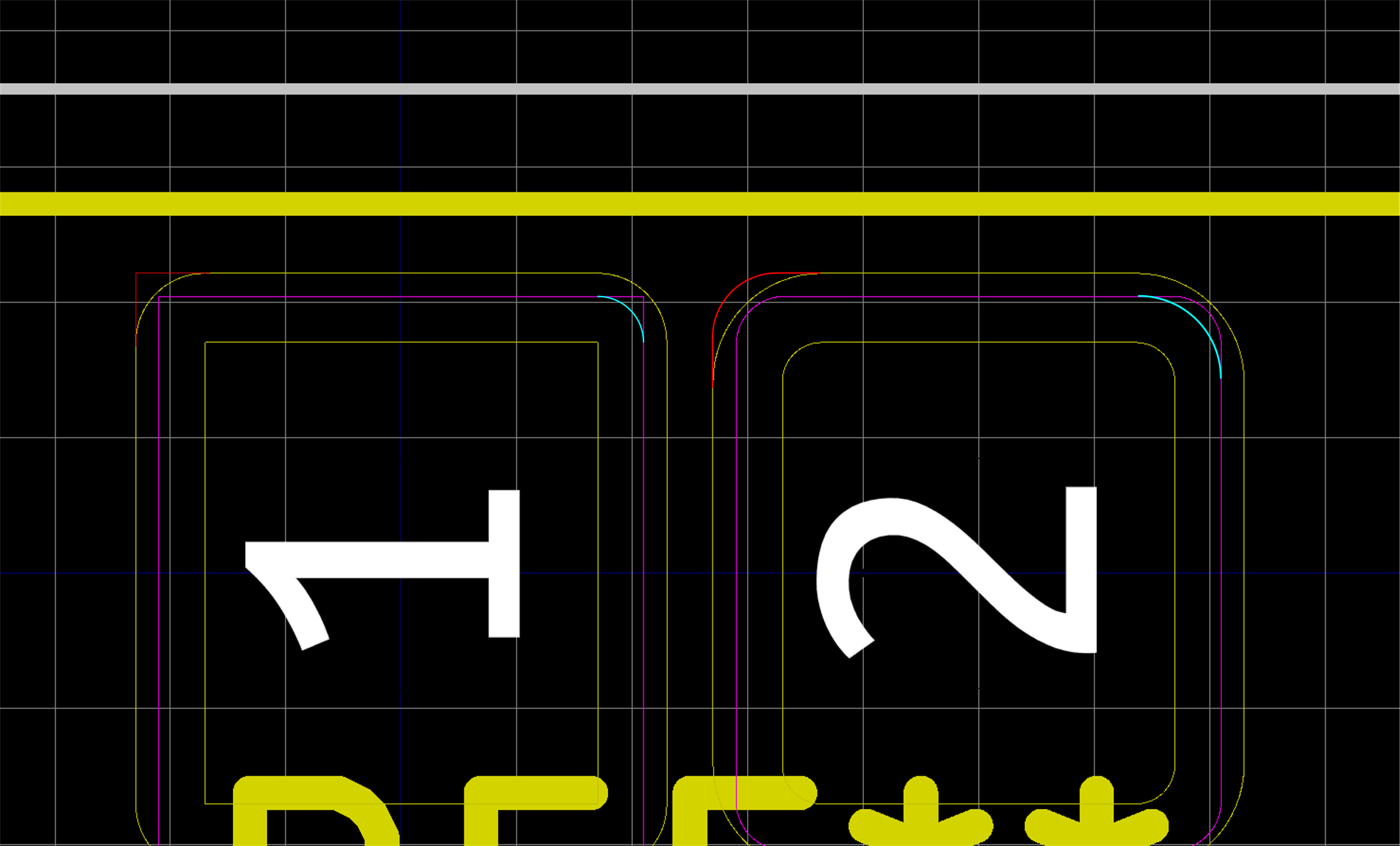
If you place an SMT pad in a zone, due to the way the zone clearance gets rounded corners it can mean there's a little bit of copper that overlaps into the pad area.
For example: the attached screenshot shows a zone of clearance 0.01in inside which is placed an SMT pad of mask clearance just under 0.008in (the actual value 0.007874015748in being 0.2mm). You would expect that this is perfectly safe; a nice 0.002in of safety margin between the solder mask opening and the copper zone.
But you'd be wrong. The problem is that the zone clearance only applies vertically and horizontally from the pad; the cleared area within the zone gets a rounded corner of radius 0.010in, meaning it could only guarantee clearance of a square corner at most 0.00707...in (0.01in * sqrt(2)) wide. The mask clearance of 0.008in gives a tiny margin of bare copper from the filled zone exposed within the pad clearance area.
This isn't just a rendering issue; I have had a bad copper run of boards from the fab because of actual spilled out copper in these pad areas, causing grounding shorts to the pads when soldered.
As a workaround for these collisions I've been manually editing the per-pad Cu clearance settings and increasing it on any pad that would be affected. I'd prefer to leave the global zone clearance at a nice small 0.01in though because I need to route some grounding pour between TTH connector pads, so that can't be too big.

| summary: |
- Pad-to-Zone clearance collisions at corners + Zone vs. Soldermask clearance collisions at corners |
| Changed in kicad: | |
| status: | New → Triaged |
| Changed in kicad: | |
| assignee: | nobody → Jeff Young (jeyjey) |
| status: | Triaged → In Progress |
| milestone: | none → 6.0.0-rc1 |
Please paste your version information.