pcbnew: throw exception when import pcad pcb with zero size pads

Bug #1551353 reported by Eldar Khayrullin
8
This bug affects 1 person
Affects Status Importance Assigned to Milestone
KiCad
Fix Released
Undecided
Eldar Khayrullin

Bug Description

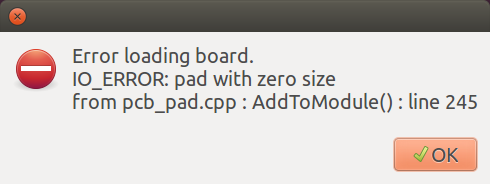
Unpossible import PCAD pcb file with zero size pads.

Application: kicad
Version: 0.201602281447+6595~42~ubuntu15.10.1-product release build
wxWidgets: Version 3.0.2 (debug,wchar_t,compiler with C++ ABI 1009,GCC 5.2.1,wx containers,compatible with 2.8)
Platform: Linux 4.2.0-30-generic x86_64, 64 bit, Little endian, wxGTK
Boost version: 1.58.0
         USE_WX_GRAPHICS_CONTEXT=OFF
         USE_WX_OVERLAY=OFF
         KICAD_SCRIPTING=ON
         KICAD_SCRIPTING_MODULES=ON
         KICAD_SCRIPTING_WXPYTHON=ON
         USE_FP_LIB_TABLE=HARD_CODED_ON
         BUILD_GITHUB_PLUGIN=ON

Tags: pcbnew pcad

Related branches

Revision history for this message
Eldar Khayrullin (eldar) wrote :
Revision history for this message
Eldar Khayrullin (eldar) wrote :

After patch

Revision history for this message
Eldar Khayrullin (eldar) wrote :
Revision history for this message
jean-pierre charras (jp-charras) wrote :

Eldar,
Your fix is not good.
A 0 sized pad will create a lot of issues and potential crashes in Pcbnew.
For a TH pad, this is even a non sense: a TH pad connects layers between layers, and this is not possible with a 0 sized pad.

You can:
- discard this pad (this is certainly the best way: I do not understand the meaning of a 0 sized pad.).
- or give it a reasonable drill value and size.

Revision history for this message
Eldar Khayrullin (eldar) wrote :

Ok. I think your first variant resolve of problem is good - discard zero pads.
0 sized pads maked maybe for don't drill them was done with lazy man who don't want edit footprint.
But this file should be opened.
I fix this when I have a time

Revision history for this message
Eldar Khayrullin (eldar) wrote :

Patch: ignore zero size pads and vias. No throw exceptions

Revision history for this message
Eldar Khayrullin (eldar) wrote :

What about status of bug?
JP, I applied your comments to patch.

Revision history for this message
jean-pierre charras (jp-charras) wrote :

Sorry, Eldar, for the delay (I just forgot your patch...).
I committed your patch in rev 6619.

Changed in kicad:
status: New → Fix Committed
Revision history for this message
Eldar Khayrullin (eldar) wrote :

All Ok. Thank you

Revision history for this message
PCB Wiz (1-pcb-wiz) wrote :

I have done many tests with KiCad and 0 size pads in June release, for a Mentor Translator

"jp-charras: A 0 sized pad will create a lot of issues and potential crashes in Pcbnew.
For a TH pad, this is even a non sense: a TH pad connects layers between layers, and this is not possible with a 0 sized pad.

I use a Zero Size Cu PAD, with a Finite Drill, to carry Drill info, and add F.Cu and B.Cu pads to carry the actual copper shape.
This approach allows kiCad to support different sizes/rotations on F/B, and allows slot rotate too.
That covers most possible Mentor PADS PadStacks.

Tests show :
KiCad can load and save zero size pads, without crashes.
There is one niggling pour+thermal DRC issue, but I think that actually _needs_ a zero size pad in KiCad to solve.

" eldar: 0 sized pads maked maybe for don't drill them was done with lazy man who don't want edit footprint."

In Mentor releases, the 0 Size PADS is actually common, which is another reason it should be supported.

It is used as something of a workaround in cases of
a) Vertical and Horiz TO220. Mentor rules mandated equal pad-count on alternate decals, but V=3,H=4.
the solution is to have 4th 0 Size pad on V.
b) Pin number skipping - Older versions that needed sparse DIP numbering used 0 Size pads to skip numbers.

Newer Mentor releases I think now allow Alternates with differing Pin counts, and a new AlphaNumber scheme
allows eg 1,7,8,14 on a DIP4 - however, there will be plenty of old-database designs out there, that will use the 0 size entity.

My suggestion would be to keep the P-CAD skip-0 patch, until the fill+thermal connectivity DRC fail detail is resolved, and then, when I have tested Mentor imports, it should be safe to re-enable the PAD Size 0 in PCAD.

Changed in kicad:
status: Fix Committed → Fix Released
Revision history for this message
Eldar Khayrullin (eldar) wrote :

To PCB Wiz, open new bug (like Zero sized pads) and add it to Wishlist

To post a comment you must log in.
This report contains Public information  
Everyone can see this information.

Other bug subscribers

Remote bug watches

Bug watches keep track of this bug in other bug trackers.