KiCad fills copper areas from BRD-files differently than Eagle
| Affects | Status | Importance | Assigned to | Milestone | |
|---|---|---|---|---|---|
| KiCad |
Fix Committed
|
Low
|
Seth Hillbrand | ||
Bug Description
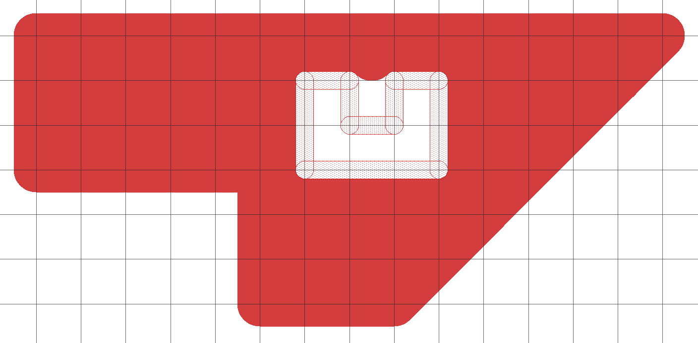
When filling a copper area in Eagle, the line width the copper area is drawn with is taken into account so the filled area is bigger than the drawn polygon by the radius of the line used to draw it (in all directions).
When I import the board-file into KiCad, as far as I can tell the line used to draw the copper area has no line width and thus the middle of the polygon line is taken as outer contour when calculating the fill. This leads to ugly areas different than what my customers tried to make.
(I am an absolute beginner in both KiCad and Eagle so my interpretation could be wrong.)
Application: kicad
Version: (5.0.0), release build
Libraries:
wxWidgets 3.0.3
libcurl/7.54.1 OpenSSL/1.0.2l zlib/1.2.11 libssh2/1.8.0 nghttp2/1.23.1 librtmp/2.3
Platform: Windows 7 (build 7601, Service Pack 1), 64-bit edition, 64 bit, Little endian, wxMSW
Build Info:
wxWidgets: 3.0.3 (wchar_t,wx containers,
Boost: 1.60.0
OpenCASCADE Community Edition: 6.8.0
Curl: 7.54.1
Compiler: GCC 7.1.0 with C++ ABI 1011
Build settings:
USE_
USE_
KICAD_
KICAD_
KICAD_
KICAD_
BUILD_
KICAD_
KICAD_
KICAD_SPICE=ON

| tags: | added: eagle import pcbnew |
This might be related: https:/