Pcbnew: improve text and layer options, esp. for boards which use bare copper as heat sinks.

Bug #1783249 reported by Gabriel Staples
22
This bug affects 5 people
Affects Status Importance Assigned to Milestone
KiCad
Confirmed
Wishlist
Unassigned

Bug Description

Application: kicad
Version: 5.0.0-fee4fd1~65~ubuntu14.04.1, release build
Libraries:
    wxWidgets 3.0.2
    libcurl/7.35.0 OpenSSL/1.0.1f zlib/1.2.8 libidn/1.28 librtmp/2.3
Platform: Linux 4.4.0-112-generic x86_64, 64 bit, Little endian, wxGTK
Build Info:
    wxWidgets: 3.0.2 (wchar_t,wx containers,compatible with 2.8) GTK+ 2.24
    Boost: 1.54.0
    OpenCASCADE Community Edition: 6.8.0
    Curl: 7.35.0
    Compiler: GCC 4.8.4 with C++ ABI 1002
Build settings:
    USE_WX_GRAPHICS_CONTEXT=OFF
    USE_WX_OVERLAY=OFF
    KICAD_SCRIPTING=ON
    KICAD_SCRIPTING_MODULES=ON
    KICAD_SCRIPTING_WXPYTHON=OFF
    KICAD_SCRIPTING_ACTION_MENU=ON
    BUILD_GITHUB_PLUGIN=ON
    KICAD_USE_OCE=ON
    KICAD_USE_OCC=OFF
    KICAD_SPICE=ON

-----------------------------------------

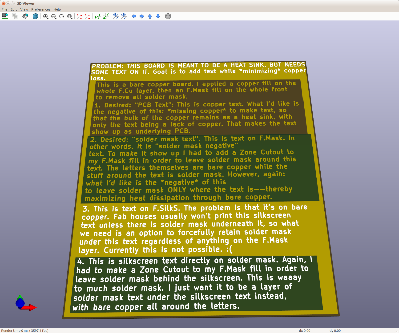
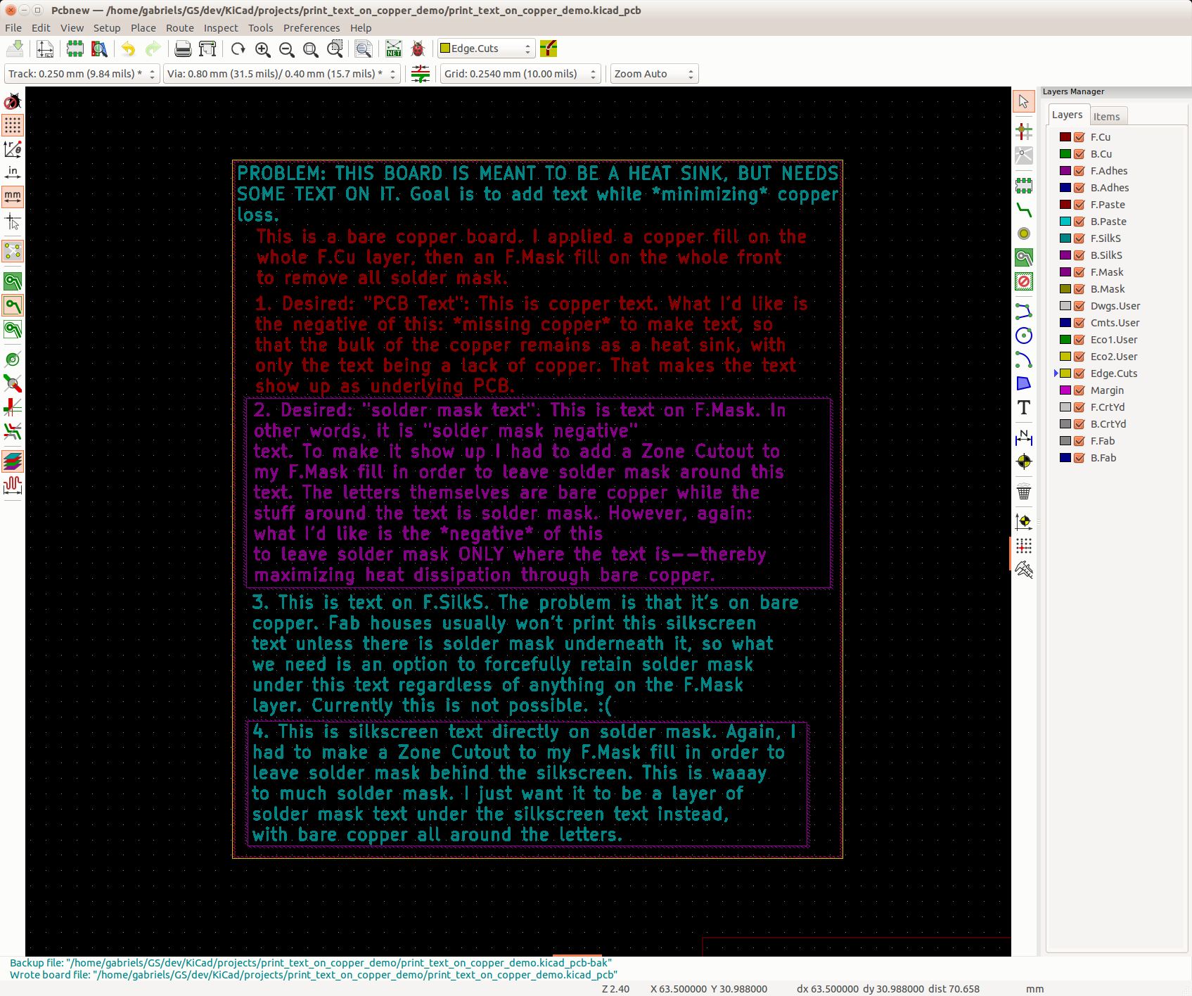
TLDR; see 2 attached images in the next posts below.

Request: Pcbnew: allow printing text in solder mask, not just solder mask negative, and in copper negative, not just copper, and make a “forcefully retain solder mask under text” option when text is on silkscreen layer, & a "negative" option for text on all layers.

Details:

I'd like to make text out of solder mask, but this is currently impossible in KiCad. Let me explain. Let me also add this is a really important feature for me, so I hope you decide to implement it.

From an email I sent to Osh Park:
"I have a board I have intentionally removed solder mask from in many areas in order to make the whole board a heat sink. I'd still like silkscreen, however, on these areas. Can you print silkscreen onto copper (without solder mask there)?"

Their response:
"The fab will automatically remove silkscreen which is not directly on top of solder mask. This is done to prevent accidentally applying silkscreen over pads, which would cause soldering issues.
The usual solution in this situation is to leave a block of solder mask under the area to which you would like to apply silkscreen. Since the solder mask is quite thin, only ~1 mil thick (0.025 mm), it also may not significantly restrict heat flow where applied."

But....this is impossible in KiCad.
Please add an option to “forcefully retain solder mask under text” option when text is on silkscreen layer. Make this override any Mask layers, such as F.Mask or B.Mask.

I'd also like to write in copper negative on top of bare copper. In other words, I can apply an F.Mask zone to remove all solder mask, and I can add a copper fill, then I can place text on the F.Cu layer. However, the text doesn't show up unless I add a cutout zone on the copper fill layer around the text, since the text is copper. Please add a "make negative" button whenever we place text on any layer, to invert the text. This would allow me to write text onto a copper fill by making the text show up as places where copper is *not* present.

From my question here: https://forum.kicad.info/t/how-can-i-write-text-in-solder-mask/11587
"I’d like to write text in solder mask by using the F.Mask layer. However, there seems to be no way to make this a negative. In other words, I can easily add text to the F.Mask layer, but that leaves solder mask as the background and makes the text now uncovered copper, but what I want to do is the opposite: I’d like to leave the background as uncovered copper and make the text solder mask.
See the attached image from the KiCad 3D viewer. Yellow is bare copper and green is solder mask. I’d like the negative of this. Any way to do it?"

Tags: pcbnew
summary: Pcbnew: allow printing text in solder mask, not just solder mask
negative, and in copper negative, not just copper, and make a
“forcefully retain solder mask under text” option when text is on
- silkscreen layer
+ silkscreen layer, & a "negative" option for text on all layers.
description: updated
Revision history for this message
Gabriel Staples (ercaguy) wrote :

TLDR; see attachments.

summary: - Pcbnew: allow printing text in solder mask, not just solder mask
- negative, and in copper negative, not just copper, and make a
- “forcefully retain solder mask under text” option when text is on
- silkscreen layer, & a "negative" option for text on all layers.
+ Pcbnew: improve text and layer options, esp. for boards which use bare
+ copper as heat sinks.
Revision history for this message
Gabriel Staples (ercaguy) wrote :

TLDR; see attached images.

description: updated
Revision history for this message
Gabriel Staples (ercaguy) wrote :

See this attached image for what I want the text to do. It will literally look like this (as shown in the 3D board image)---with bare copper all around, but the text itself will be made up of different things:
1. Bare PCB with no copper, but copper all around each character.
2. Solder mask, with copper all around each character.
3. Silkscreen with underlying solder mask, with copper all around each character.

These would be fantastic text & layer additions and would make heat-sink PCBs much more possible and practical in KiCad. Frequently, it is helpful to expose parts of the board's copper to dissipate heat better, but the area still might be needed for helpful text or other silkscreen, so that's what I'm trying to get.

Don't forget though: this should apply to graphic lines and things too, not just text.

Revision history for this message
PCB Wiz (1-pcb-wiz) wrote :

See also the older
https://bugs.launchpad.net/kicad/+bug/1463857

My suggested way to manage this, is to simply allow multiple layer plot selections.

Easy to explain, and many variant uses are possible.

User selects layer (usually 1) to PLOT DARK.
Then they select layer (usually 1) to PLOT CLEAR, and the plot routine appends the second gerber, with the %LPC% command header.

Of course, this is user-beware stuff, and any LPC WILL blindly 'cut into' what you already have, so this MUST be checked in GerbView, that it really did what user hoped :)

Revision history for this message
Gabriel Staples (ercaguy) wrote :

Any thoughts from the developers on how you feel about this issue, or when it might be implemented? Even if you triage it for later down the road, I still feel it would be a very welcome and useful addition.

Meanwhile, I can forcefully retain solder mask under silkscreen, to allow "printing silkscreen on bare copper", using bobc's python script to modify the gerbers as follows: `~/dev/KiCad/utilities/bobc/kicad-utils/scripts/gerber_combine/gerber_combine.py myBoard-F.Mask.gbr -s myBoard-F.SilkS.gbr -o myBoard-F.Mask_NEW.gbr`. This subtracts the F.SilkS layer from the F.Mask layer, thereby forcing solder mask to remain under all silkscreen. It's an okay work-around for now, but it would be much better if it was all doable inside Pcbnew. Then it would be easier, faster, and we'd be able to see everything rendered nicely in the 3D viewer.

tags: added: pcbnew
Jeff Young (jeyjey)
Changed in kicad:
importance: Undecided → Wishlist
status: New → Confirmed
Revision history for this message
Jeff Young (jeyjey) wrote :

I think doing anything automated would be too complicated and error-prone (from a user's perspective, not from a code perspective).

Once we have knock-out text you could simply place two text objects: one knock-out on the mask layer, and one regular on the silkscreen layer. Yes, you'd have to make sure they had identical text and were at identical locations, but at least it would be clear that the user is driving and needs to ensure that their Gerbers look like what they want.

I'm therefore closing this as a duplicate of knock-out text. (I'll also put a comment in that bug to refer to it.)

To post a comment you must log in.
This report contains Public information  
Everyone can see this information.

Other bug subscribers

Remote bug watches

Bug watches keep track of this bug in other bug trackers.