Clearances not enforced on filled zones (under estimates)

Bug #1735206 reported by Jt Whissel
6
This bug affects 1 person
Affects Status Importance Assigned to Milestone
KiCad
Fix Released
Undecided
Unassigned

Bug Description

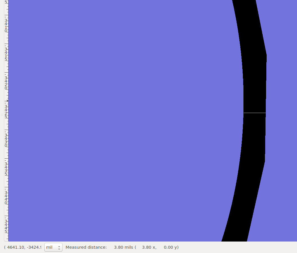
The clearance for this top layer ground fill is set to 4mil There are several spots (this was the worst one I could find) that the clearance is not respected. If it should go above the clearance limit but should never go under. This can cause manufacturing issues, higher manufacturing costs (if you're under 4 then you pop into the 3mil tier, etc).

Application: kicad
Version: no-vcs-found-0564d34~61~ubuntu17.10.1, release build
Libraries:
    wxWidgets 3.0.3
    libcurl/7.55.1 OpenSSL/1.0.2g zlib/1.2.11 libidn2/2.0.2 libpsl/0.18.0 (+libidn2/2.0.2) librtmp/2.3
Platform: Linux 4.13.0-17-generic x86_64, 64 bit, Little endian, wxGTK
Build Info:
    wxWidgets: 3.0.3 (wchar_t,wx containers,compatible with 2.8) GTK+ 2.24
    Boost: 1.62.0
    Curl: 7.55.1
    Compiler: GCC 7.2.0 with C++ ABI 1011

Build settings:
    USE_WX_GRAPHICS_CONTEXT=OFF
    USE_WX_OVERLAY=OFF
    KICAD_SCRIPTING=ON
    KICAD_SCRIPTING_MODULES=ON
    KICAD_SCRIPTING_WXPYTHON=ON
    KICAD_SCRIPTING_ACTION_MENU=ON
    BUILD_GITHUB_PLUGIN=ON
    KICAD_USE_OCE=ON
    KICAD_SPICE=ON

Tags: drc
Revision history for this message
Jt Whissel (jtwhissel) wrote :
Revision history for this message
Nick Østergaard (nickoe) wrote :

Could you please attach the kicad_pcb file which shows this violation?

tags: added: drc
removed: clearance filled zones
Revision history for this message
Jt Whissel (jtwhissel) wrote :

Unfortunately I can not since it's not mine to share (I use Kicad professionally). However, I did my best to make a sample board of the problem. It shows off the trace to fill clearance issue and the fill to self-fill clearance issue.

Revision history for this message
Nick Østergaard (nickoe) wrote :

Thank you, that should be good.

Revision history for this message
jean-pierre charras (jp-charras) wrote :

I am afraid your understatement of "clearance" is wrong.

The board has only one zone defined (with no netname).

A clearance has meaning only between objects belonging 2 different nets (this is not the case here).
One cannot define a clearance between 2 objects of the same net, because they are expected to be connected, therefore most of times the clearance is (obviously) 0.

It is unlikely we can fix your problem.

Revision history for this message
jean-pierre charras (jp-charras) wrote :

"I am afraid your understatement"
Please, read:
I am afraid your understanding ...

Sorry.

Changed in kicad:
status: New → Invalid
Jt Whissel (jtwhissel)
Changed in kicad:
status: Invalid → New
Revision history for this message
Jt Whissel (jtwhissel) wrote :

New evidence of the problem happening with two different nets as well. Should round up instead of down.

Revision history for this message
Jt Whissel (jtwhissel) wrote :

This is measured in gEDA Gerber viewer. The measured distance is at the bottom right. clearance is set to 4 mils.

Revision history for this message
Jt Whissel (jtwhissel) wrote :

Here is the kicad file, the clearance issue is on the right side of the first pad hole to ground.

Revision history for this message
KiCad Janitor (kicad-janitor) wrote :

Fixed in revision 673f03e59525a6cdfd97739906d50c9510a94d0d
https://git.launchpad.net/kicad/patch/?id=673f03e59525a6cdfd97739906d50c9510a94d0d

Changed in kicad:
status: New → Fix Committed
Changed in kicad:
status: Fix Committed → Fix Released
To post a comment you must log in.
This report contains Public information  
Everyone can see this information.

Other bug subscribers

Remote bug watches

Bug watches keep track of this bug in other bug trackers.