pcbnew: Add via types and zones to displayed items list

Bug #1796118 reported by Victor W
16
This bug affects 3 people
Affects Status Importance Assigned to Milestone
KiCad
Expired
Wishlist

Bug Description

I'm using one of the latest nightly PCBnew versions.

PROBLEM:

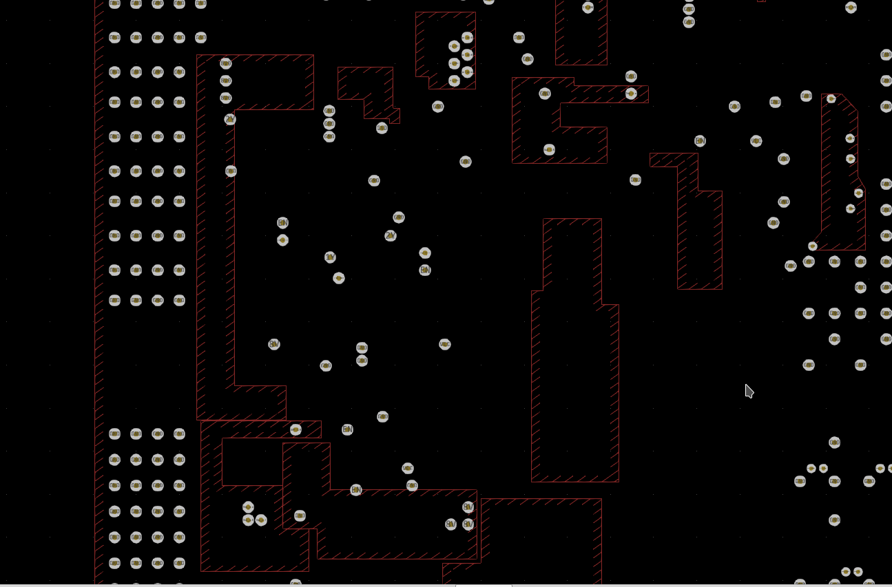
Some items are only displayed if the top copper layer is also displayed.

For example, I can't only show through hole vias without also showing tracks.

PROBLEM:

I expect that if I hide all copper layers and items, except for, say, footprint front, then I should just see all the footprints.

ACTUAL:

Using the layer manager, and on the Layers tab, I right click to hide all layers. Then, I go to the items tab I expect that if I hide footprints, and only have through hole vias selected, that I will only see the Vias on the screen.

Similarly, if I hide vias, and only want to see front foot prints, then I should be able to hide all tracks, and only see footprints, or vias, or other items.

RESULT:

What actually happens is that I can only see the vias if I also have a copper layer selected. If there is no copper layer selected, then I can't see any of the objects.

I kind of understand how this might make sense - if you don't have any copper layers selected, then presumably everything should be hidden. But the the problem is that I can't figure out how to only show footprints without any other copper, or how to only show vias without any other traces.

EXPECTED:

That if I unselect all copper layers, and only have specific items selected, then that's all I will see. This appears to work for copper layers (I can set things up so I only see tracks, and no pads or vias), but doesn't seem to work for items (I can't figure out how to set things up so I only see items, without tracks).

====

Application: kicad
Version: (6.0.0-rc1-dev-673-g3a9e7a496), release build
Libraries:
    wxWidgets 3.0.4
    libcurl/7.61.1 OpenSSL/1.1.1 zlib/1.2.11 libidn2/2.0.5 libpsl/0.20.2 (+libidn2/2.0.4) nghttp2/1.33.0
Platform: Linux 4.18.9-arch1-1-ARCH x86_64, 64 bit, Little endian, wxGTK
Build Info:
    wxWidgets: 3.0.4 (wchar_t,wx containers,compatible with 2.8) GTK+ 2.24
    Boost: 1.68.0
    OpenCASCADE Community Edition: 6.9.1
    Curl: 7.61.1
    Compiler: GCC 8.2.1 with C++ ABI 1013

Build settings:
    USE_WX_GRAPHICS_CONTEXT=OFF
    USE_WX_OVERLAY=OFF
    KICAD_SCRIPTING=ON
    KICAD_SCRIPTING_MODULES=ON
    KICAD_SCRIPTING_WXPYTHON=OFF
    KICAD_SCRIPTING_ACTION_MENU=ON
    BUILD_GITHUB_PLUGIN=ON
    KICAD_USE_OCE=ON
    KICAD_USE_OCC=OFF
    KICAD_SPICE=ON

Victor W (vicw)
description: updated
Revision history for this message
Seth Hillbrand (sethh) wrote :

Does unchecking the "Tracks" item not give you what you want?

Revision history for this message
Seth Hillbrand (sethh) wrote :

Attaching an image to show options.

Here I have only F.Cu selected in the Layers tab.

Revision history for this message
Victor W (vicw) wrote :

Dear Seth,

Thanks for point that out - it gets me half of the way there, though I realize I didn't accurately write up the initial report.

I should have included zones in the mix and been more specific in noting that I can't configure things to hide via's, and only see tracks and pours, but I can't set things up so that I ONLY see vias, if I also have zones on a layer.

If you add a polygon pour to your examples, I can't figure out how to hide it. For what we do, it's nice if I can separate copper tracks and pours from vias. It's straightforward to only show tracks and zones, without vias, but I can't seem to figure out how to only show vias, if I also have zones.

I feel I must be missing something; I feel like maybe I'm not seeing a box for "zone" or "drawing" items.

Revision history for this message
Victor W (vicw) wrote :

(Sorry the previous post had a typo;

I *CAN* configure PCBnew to view copper tracks and pours for a specific layers (and hide vias).

I *CANNOT* figure out how to configure PCBnew to ONLY show vias, but NOT copper zones, keep-outs, or drawings for a given layer.

Revision history for this message
Seth Hillbrand (sethh) wrote :

You can change the zone display on the left hand side so that you don't see the copper fill.

Does this address your use case?

Revision history for this message
Victor W (vicw) wrote :

It doesn't quite help; that only puts them in outline mode; I can't seem to hide them completely.

(NOTE: It's similar to how you can't differentiate between micro vias and blind/buried vias. When we do design reviews, we focus on complex geometries, and it would be nice to be able to separately show blind/buried vias). Right now, we just look for the special colour and it works out.

I am attaching a modified screen shot that shows some of the area I am trying to copy.

The current work-around is to switch to a ground layer, put it in outline mode, and set things up so that only the desired vias are present.

Ideally, though, I'd be able to separately and completely hide and show those zones so I can just select the entire region without having to switch layers.

Revision history for this message
Seth Hillbrand (sethh) wrote :

OK, that makes sense. I think that this is a wishlist item for two separate things:

1) Put a show/hide zones checkbox in the items list

2) Add distinguishing features to the blind/buried vias (like a to/from bi-color thing) to distinguish them.

Is this a correct summary?

Revision history for this message
Victor W (vicw) wrote :

I think that's an excellent summary for the first issue (showing/hiding zones).

The blind/buried vias are already distinguished by special colouring - they already have a special colour pattern that makes it easy to identify what layers they connect (though one a colour blind engineer needs to modify the layer colouring to make it easier to see). Just put them in the item list;

2) Put a "show/hide buried vias" check box in the items list.

3) Put a "show/hide blind vias" check box in the items list.

I suppose the real issue here relates to expectations; all the other item types can be controlled through the item manager independently from any other item type and layer. My own expectation was that I could control the visibility of everything separately. For example, I can toggle the visibility of through vias separately from NPTH. And I can select tracks separately from pads...

EXCEPT when it comes to zones, blind vias, and buried vias.

The reason I want to hide these things is to make my life easier when I copy/paste...

For example, when you are in high contrast mode and on an active layer, and if you want to copy a region, the tracks and elements on other layers are ignored, and can't be selected (exactly as you would want and expect), EXCEPT for the buried vias - even if the specific layer you are copying falls above or below the specific via path.

Again, this isn't a show stopper. Our current work around is to first copy it outside the PCB, double check and delete any elements we don't want, and then copy that pattern and put it where we need it to go.

Seth Hillbrand (sethh)
summary: - PCBnew: Unable to only show Vias
+ pcbnew: Add via types and zones to displayed items list
Changed in kicad:
importance: Undecided → Wishlist
status: New → Triaged
Revision history for this message
eelik (eelik) wrote :

Possible solution which doesn't break existing workflows or behavior:

Add "Invert layer/item visibility logic" checkbox to Layers Manager -> Items list. That would invert the logic so that visibility logic would work like this:

1. Layers->Copper layer is unselected. So, start from "no items visible".
2. Also Fab and Silk layers (for references etc.) are unselected.
2. Items->Footprints is unselected. So, continue with "no footprints visible".
3. Items->References is selected. So, *show* references of footprints.
4. Items->Pads Front is selected. So, show front pads.
5. Items->Through Via is selected. So, show vias.

The result: only front pads, references and vias are visible. No other copper, silk or fab items (which are unselected).

Revision history for this message
eelik (eelik) wrote :

Hmm... the previous comment relates to the original question (about visibility locig), not to the changed subject line.

Actually I would like to see Zones in the visibility list. That would have a nice side effect that I could change the opacity of zones and lessen the need to switch between outline and filled modes. I often tweak positions of tracks and vias after everything is othewise ready so that I can have better filled areas. But it's a bit difficult because tracks get lost inside filled zones. I could keep the zones in filled mode all the time if I could see through them.

Revision history for this message
NhatKhai (nhatkhai) wrote :

Looking like https://bugs.launchpad.net/kicad/+bug/1811355 also relative to this.

Revision history for this message
Steven Slupsky (sslupsky) wrote :

I agree with @eelik regarding having zones in the items visibility list. It is mostly a convenience thing since you can turn the zone visibility on and off on the other side of the window.

Another item I would like to highlight is the ability to see the through hole pads from the opposite side of the board. This is an issue when placing reference designators on the silkscreen layers. For instance, silkscreen on the bottom layer. If I have a footprint placed the top layer that has through hole pads, when I turn off the "Footprints front", the through pads disappear. So, if I am placing reference designators on the the bottom layer, I cannot see the through pads to avoid placing the silkscreen over top of the pads.

Jon Evans (craftyjon)
Changed in kicad:
assignee: nobody → Jon Evans (craftyjon)
Revision history for this message
KiCad Janitor (kicad-janitor) wrote :

KiCad bug tracker has moved to Gitlab. This report is now available here: https://gitlab.com/kicad/code/kicad/-/issues/2254

Changed in kicad:
status: Triaged → Expired
To post a comment you must log in.
This report contains Public information  
Everyone can see this information.

Other bug subscribers

Remote bug watches

Bug watches keep track of this bug in other bug trackers.