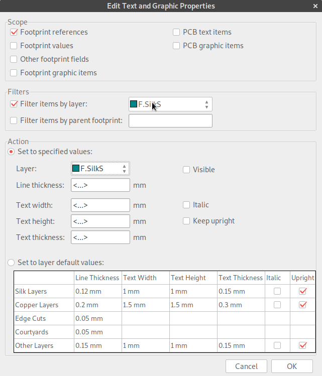
feature to swap values for reference onto silk screen
Bug #1793429 reported by
zakhar nasimov
This bug affects 2 people
| Affects | Status | Importance | Assigned to | Milestone | |
|---|---|---|---|---|---|
| KiCad |
Fix Released
|
Wishlist
|
Unassigned | ||
Bug Description
Currently if one prefers to have values on the silk per component instead of reference they must swap them one by one manually or modify the footprint.
This bug is a feature request to implement functionality to permit Eeschema to place values onto silk layer for PCBNew instead of reference being on silk layer if desired by the user.
| summary: |
- feature to swap layer objects to other layers especially value to - reference + feature to swap values for reference onto silk screen |

| Changed in kicad: | |
| status: | New → Triaged |
| importance: | Undecided → Wishlist |
| Changed in kicad: | |
| status: | Fix Committed → Fix Released |
To post a comment you must log in.
This would be nice, specially for testpoints.
Also note that even if you move the value of a footprint to the Silks layer they are not included in
the corresponding gerber layer or 3d view.